README.md
# Standard JST programmer
Use a three-pin JST SH (1 mm) connector for SWD with separate two-pin power, or use the five-pin connector for SWD, power, and NRST in one cable. The SWD connector follows the [Raspberry Pi Debug Connector pinout](https://datasheets.raspberrypi.com/debug/debug-connector-specification.pdf).
The three-pin interface can also be used for **Spy-Bi-Wire (SBW)** with compatible programmer firmware. See [Spy-Bi-Wire wiring and firmware requirements](#use-spy-bi-wire-sbw).
## Install
```sh
tsci add tscircuit/standard-jst-programmer
```
## Choose components
| Export | Use |
| --- | --- |
| `StandardJstSwdUpward` | Upward-facing three-pin SWD connector. Also the default export. |
| `StandardJstSwdSide` | Side-facing three-pin SWD connector. |
| `StandardJstUartUpward` | Upward-facing three-pin UART target connector, with RX/GND/TX silkscreen. |
| `StandardJstUartSide` | Side-facing three-pin UART target connector, with RX/GND/TX silkscreen. |
| `StandardJstPowerUpward` | Upward-facing two-pin power connector. |
| `StandardJstPowerSide` | Side-facing two-pin power connector. |
| `StandardJstSwdResetUpward` | Upward-facing five-pin SWD, power, and NRST drop-in. |
| `StandardJstSwdResetSide` | Side-facing five-pin SWD, power, and NRST drop-in. |
| `StandardTagConnectSwd` | Bare-pad TC2030 no-legs target footprint for the TC2030-IDC-NL-050 cable. |
| `ProgrammerBoard` | Complete 26 × 42 mm USB-C programmer; four copper layers, top-side assembly. |
Each JST connector includes its footprint, JLCPCB part number, and 3D model. The Tag-Connect target is bare copper and alignment holes: no purchased connector is required. Choose the three-pin interface for Raspberry Pi Debug Probe cable compatibility, or the five-pin extension when you also need NRST.
## Add SWD and power to a target board
```tsx
import {
StandardJstSwdUpward,
StandardJstPowerUpward,
} from "@tsci/tscircuit.standard-jst-programmer"
export default () => (
<board width={30} height={20}>
<StandardJstSwdUpward name="J_DEBUG" pcbX={-5} pcbY={5} />
<StandardJstPowerUpward name="J_POWER" pcbX={5} pcbY={5} />
<trace from=".J_DEBUG > .SWCLK" to="net.SWCLK" />
<trace from=".J_DEBUG > .GND" to="net.GND" />
<trace from=".J_DEBUG > .SWDIO" to="net.SWDIO" />
<trace from=".J_POWER > .VOUT" to="net.TARGET_POWER_IN" />
<trace from=".J_POWER > .GND" to="net.GND" />
{/* Add your MCU and power circuit. Connect SWCLK/SWDIO through
100 ohm series resistors placed close to the target MCU. */}
</board>
)
```
Connect `TARGET_POWER_IN` to the appropriate supply input on your target: a 3.3 V rail when selecting **3V3**, or a 5 V-rated input/regulator when selecting **5V**. Omit the power connector if the target has its own supply. Connectors do not connect to global nets automatically.
For side entry, substitute `StandardJstSwdSide` and `StandardJstPowerSide`; the electrical pin assignments stay the same. At `pcbRotation={0}`, side-entry connectors open toward −Y. Rotate 90° for +X, 180° for +Y, or 270° for −X.
All eight connector components accept placement props including `pcbX`, `pcbY`, `pcbRotation`, `schX`, and `schY`. The package exports `SwdConnectorProps`, `PowerConnectorProps`, `SwdResetConnectorProps`, and `UartConnectorProps` types.
## Add UART to a target board
```tsx
import { StandardJstUartSide } from "@tsci/tscircuit.standard-jst-programmer"
export default () => (
<board width={25} height={20}>
<StandardJstUartSide name="J_UART" pcbX={0} pcbY={-6} />
<trace from=".J_UART > .RX" to="net.MCU_UART_RX" />
<trace from=".J_UART > .GND" to="net.GND" />
<trace from=".J_UART > .TX" to="net.MCU_UART_TX" />
{/* Add the MCU and 100-ohm series resistors close to its UART pins. */}
</board>
)
```
Use `StandardJstUartUpward` for top entry. Both components reuse the verified
three-pin JST SH footprint and matching part/model (side C160403; upward C160389).
The RX, GND, and TX labels are embedded beside the corresponding contact pads;
they follow `pcbX`, `pcbY`, and `pcbRotation` automatically. Add a UART legend next
to the connector to distinguish it from SWD.
Labels describe signals from the local board's perspective. The default
`role="target"` follows the [Raspberry Pi UART connector specification](https://datasheets.raspberrypi.com/debug/debug-connector-specification.pdf).
Use `role="host"` on a programmer; it swaps TX/RX selectors and printed labels.
| Contact | Target (default) | Programmer (`role="host"`) |
| --- | --- | --- |
| 1 | RX input | TX output |
| 2 | GND | GND |
| 3 | TX output | RX input |
A straight-through JST SH cable connects programmer TX to target RX and target
TX to programmer RX. Do not cross the cable wires as well. J5 on `ProgrammerBoard`
is the host variant: UART1 GPIO8 TX and GPIO9 RX, each through 100 ohms. Logic is
fixed at 3.3 V regardless of the power-selector setting. This port has no power
pin, RTS, or CTS; connect a powered target with compatible logic levels.
Flash firmware built from this source revision (`bash firmware/build.sh`); the
older v0.5.0 UF2 does not bridge J5. USB exposes UART as CDC0 ("CDC-ACM UART
Interface") and power telemetry as CDC1 ("Target power telemetry"). Open the UART
port with DTR enabled and select the target's baud/parity/data/stop settings;
115200 8N1 is the initial setting. Identify ports by interface description rather
than assuming a COM or tty number. SWD, UART, and telemetry can operate together.
The updated layouts are shown below; the UART signal labels are part of each
reusable connector footprint.


## Add the five-pin drop-in
```tsx
import { StandardJstSwdResetSide } from "@tsci/tscircuit.standard-jst-programmer"
export default () => (
<board width={30} height={20}>
<StandardJstSwdResetSide name="J_DEBUG" pcbX={0} pcbY={-7} />
<trace from=".J_DEBUG > .VOUT" to="net.TARGET_POWER_IN" />
<trace from=".J_DEBUG > .SWDIO" to="net.SWDIO" />
<trace from=".J_DEBUG > .GND" to="net.GND" />
<trace from=".J_DEBUG > .SWCLK" to="net.SWCLK" />
<trace from=".J_DEBUG > .NRST" to="net.NRST" />
{/* Add the MCU, power circuit, and target-side SWD series resistors. */}
<resistor name="R_RESET" resistance="10k" footprint="0402"
connections={{pin1:"net.NRST", pin2:"net.V3V3"}} />
</board>
)
```
Use `StandardJstSwdResetUpward` for top entry. Connect `NRST` to the MCU's active-low reset (`RUN` on RP2040) and provide a pull-up to the target's **3.3 V logic rail**, never the selectable 5 V supply. The programmer drives reset open-drain through 100 Ω. `.nRESET` is an alias for `.NRST`.
| Five-pin contact | Selector | Target connection |
| --- | --- | --- |
| 1 | `.VOUT` | Selected 3.3 V / 5 V supply input |
| 2 | `.SWDIO` | SWD data |
| 3 | `.GND` | Ground |
| 4 | `.SWCLK` | SWD clock |
| 5 | `.NRST` | Active-low reset, with a target-side 3.3 V pull-up |
Use a straight-through five-way JST SH cable. Pin 1 follows the voltage switch; it is **not fixed at 3.3 V**. This five-pin extension is not the Raspberry Pi three-pin connector standard.
## Use a Tag-Connect cable
The programmer's **J4 TAG** header mates with the [TC2030-IDC-NL-050](https://www.tag-connect.com/product/tc2030-idc-050-6-pin-tag-connect-plug-of-nails-spring-pin-cable-no-legs-to-6-pin-0-05-idc) cable: **6 pins, 2 × 3, 1.27 mm (0.05 inch)**. Align the IDC socket's pin-1 mark/red stripe with the programmer's **1** mark. This header is unshrouded; check its orientation before applying USB power. The 2.54 mm IDC and 10-pin Cortex cables do not fit.
```tsx
import { StandardTagConnectSwd } from "@tsci/tscircuit.standard-jst-programmer"
export default () => (
<board width={30} height={25}>
<StandardTagConnectSwd name="J_DEBUG" pcbX={0} pcbY={0}
noConnect={["V5"]} />
<trace from=".J_DEBUG > .V3_3" to="net.TARGET_POWER_IN" />
<trace from=".J_DEBUG > .SWDIO" to="net.SWDIO" />
<trace from=".J_DEBUG > .NRST" to="net.NRST" />
<trace from=".J_DEBUG > .SWCLK" to="net.SWCLK" />
<trace from=".J_DEBUG > .GND" to="net.GND" />
<resistor name="R_RESET" resistance="10k" footprint="0402"
connections={{pin1:"net.NRST", pin2:"net.V3V3"}} />
{/* Add your MCU, supply input, and target-side SWD series resistors. */}
</board>
)
```
| IDC / Tag-Connect contact | Selector | Use |
| --- | --- | --- |
| 1 | `.V3_3` | Fixed 3.3 V output |
| 2 | `.SWDIO` | SWD data |
| 3 | `.NRST` | Open-drain target reset; add a pull-up to 3.3 V |
| 4 | `.SWCLK` | SWD clock |
| 5 | `.GND` | Ground |
| 6 | `.V5` | Fixed USB 5 V output |
J4 uses a **project-specific dual-power pinout**: pin 1 supplies fixed 3.3 V and pin 6 supplies USB 5 V instead of SWO. Both rails bypass the voltage selector and current monitor; the selector and current readings apply to JST VOUT only. SWD/reset logic is always 3.3 V. Do not connect this header to a target wired for SWO on pin 6.
The example powers a 3.3 V target and leaves `.V5` unconnected. For a 5 V target input, connect `.V5` instead and leave `.V3_3` unconnected. For a separately powered target, leave both supply pins unconnected. Never join the two rails or connect them to another active supply. J4 shares the SWD/reset signals with the JST ports; connect only one target at a time.
Place `StandardTagConnectSwd` on the target's top side with the usual `pcbX`, `pcbY`, and `pcbRotation` props. It provides six 0.7874 mm pads on a 1.27 mm grid, three 0.9906 mm non-plated alignment holes, no solder paste, and a central routing keepout, following the [manufacturer's Rev B footprint](https://www.tag-connect.com/wp-content/uploads/bsk-pdf-manager/2019/12/TC2030-IDC-NL-Datasheet-Rev-B.pdf). Route each contact outward, keep unrelated tracks at least 0.508 mm from the contact pads, and keep the probe's 10.4 × 7.8 mm courtyard clear for access. Mark the footprint **DNL** in the assembly BOM. Hold the no-legs cable against the board during programming, or use a TC2030-CLIP with access to the board underside. There is no connector body to assemble or display in 3D.
## Connect the cables
| SWD pin | Selector | Target connection |
| --- | --- | --- |
| 1 | `.SWCLK` | SWD clock |
| 2 | `.GND` | Ground |
| 3 | `.SWDIO` | SWD data |
| Power pin | Selector | Target connection |
| --- | --- | --- |
| 1 | `.VOUT` | Selected supply input |
| 2 | `.GND` | Ground |
Use straight-through JST SH cables: **1→1, 2→2, 3→3** for SWD and **1→1, 2→2** for power. Check contact numbers, not wire colors. The three-pin SWD connector accepts Raspberry Pi Debug Probe SWD cables. The separate power connector is this project's extension; the Raspberry Pi Debug Probe does not supply it. For SWD, the three- and two-pin cables do not carry a separate reset signal; the five-pin cable adds it. For SBW, reset shares the DIO line as described below.
## Use Spy-Bi-Wire (SBW)
The programmer hardware can support Spy-Bi-Wire using either the three-pin or five-pin JST SH connector. Its clock and bidirectional data lines connect to RP2040 GPIO2 and GPIO3 through 100 Ω series resistors. **SBW requires firmware and a host tool that implement the SBW protocol. The linked v0.5.0 CMSIS-DAP/SWD firmware and OpenOCD configurations do not provide SBW support.** Wiring an MSP430 to the connector does not make SWD firmware speak SBW.
For an SBW-capable MSP430, wire the three-pin connector as follows:
| Three-pin contact | Existing selector | MSP430 target connection |
| --- | --- | --- |
| 1 | `.SWCLK` | `TEST / SBWTCK` — SBW clock |
| 2 | `.GND` | `DVSS / GND` |
| 3 | `.SWDIO` | `RST / SBWTDIO` — bidirectional SBW data and reset |
The `StandardJstSwdUpward` and `StandardJstSwdSide` component names and selectors stay the same; connect them to SBW nets on the target:
```tsx
<StandardJstSwdUpward name="J_SBW" pcbX={0} pcbY={0} />
<trace from=".J_SBW > .SWCLK" to="net.SBWTCK" />
<trace from=".J_SBW > .GND" to="net.GND" />
<trace from=".J_SBW > .SWDIO" to="net.SBWTDIO" />
```
Connect `SBWTCK` and `SBWTDIO` to the MCU pins shown above. Use a straight-through three-way cable and check contact numbers rather than wire colors. **In SBW, reset is carried on the DIO wire.** Do not connect the programmer's separate `.NRST` output to the same target reset pin. For a single cable carrying signals and power, use the five-pin connection below.
For the MSP430FR2433, select **3V3**, remove the target coin cell, and connect the separate power connector's pin 1 (`.VOUT`) to target VCC and pin 2 to ground. Never apply 5 V to that MCU or connect the programmer's power output across a coin cell. For a separately powered target, leave VOUT disconnected and ensure its supply is compatible with the programmer's fixed 3.3 V signal levels.
Follow the target MCU's SBW requirements for reset pull-up, reset capacitance and cable length. See [TI's MSP430 programming guide](https://www.ti.com/lit/pdf/slau320) and the [MSP430FR2433 datasheet](https://www.ti.com/lit/ds/symlink/msp430fr2433.pdf). This documents the hardware mapping; SBW operation on this board still requires suitable firmware and physical validation.
### Five-pin JST cable for SBW
Use `StandardJstSwdResetSide` or `StandardJstSwdResetUpward` on the target with a **straight-through five-way JST SH (1 mm) cable**. Four contacts are used for SBW and power; the fifth stays unconnected on the target.
| Five-pin contact | Existing selector | SBW target connection |
| --- | --- | --- |
| 1 | `.VOUT` | Target VCC; set the programmer to **3V3** for MSP430FR2433 |
| 2 | `.SWDIO` | `RST / SBWTDIO` — both SBW data and target reset |
| 3 | `.GND` | `DVSS / GND` |
| 4 | `.SWCLK` | `TEST / SBWTCK` |
| 5 | `.NRST` | **No connection** on the target |
Pin 2 connects to the MSP430's reset pin because that pin also carries SBW data. **Do not connect pin 5 to reset or bridge pins 2 and 5.** The separate NRST output is for SWD targets; SBW firmware controls reset through DIO.
```tsx
import { StandardJstSwdResetSide } from "@tsci/tscircuit.standard-jst-programmer"
export default () => (
<board width={30} height={20}>
<StandardJstSwdResetSide name="J_SBW" pcbX={0} pcbY={-7}
noConnect={["NRST"]} />
<trace from=".J_SBW > .VOUT" to="net.TARGET_VCC" />
<trace from=".J_SBW > .SWDIO" to="net.SBWTDIO" />
<trace from=".J_SBW > .GND" to="net.GND" />
<trace from=".J_SBW > .SWCLK" to="net.SBWTCK" />
{/* Add the MSP430: RST/SBWTDIO to SBWTDIO, TEST/SBWTCK to SBWTCK,
DVCC to TARGET_VCC, and DVSS to GND. Add its required bypass
capacitors and datasheet-specified reset pull-up/capacitance. */}
</board>
)
```
Use `StandardJstSwdResetUpward` for top entry with the same wiring. When powering the target through pin 1, remove its coin cell or disconnect its other supply; leave the separate two-pin power cable unplugged. For a separately powered target, omit the `.VOUT` trace and use `noConnect={["VOUT", "NRST"]}` so pins 1 and 5 are unconnected on the target. Ground must remain connected, and the target must tolerate the programmer's fixed 3.3 V signal levels.
The five-pin cable changes only the wiring: **SBW-capable firmware and a matching host tool are still required**. The SWD `openocd-reset.cfg` is not an SBW configuration.
## Use the programmer
```tsx
import { ProgrammerBoard } from "@tsci/tscircuit.standard-jst-programmer"
export default () => <ProgrammerBoard />
```
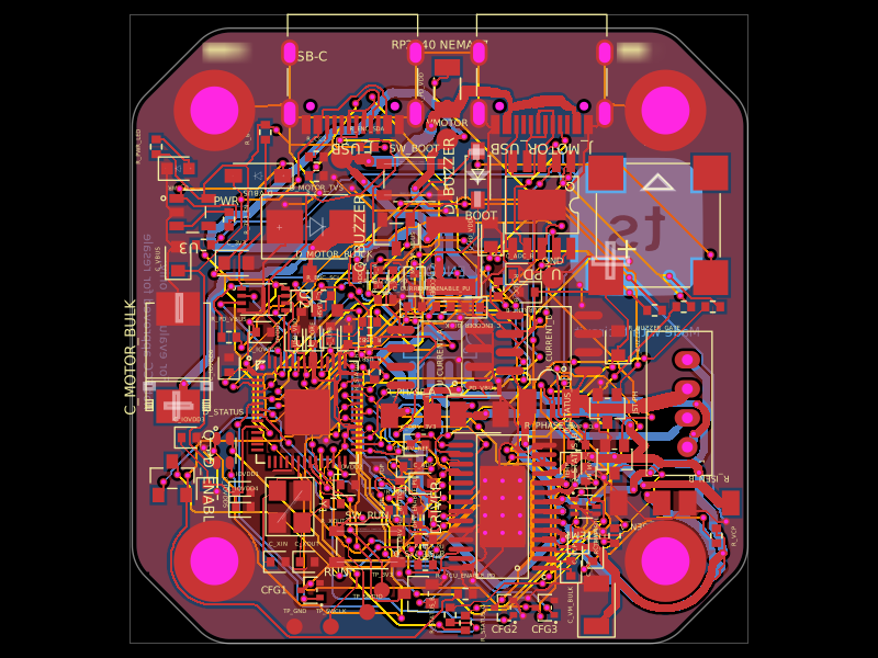
`ProgrammerBoard` contains a `<board>`; use it as the root circuit. USB-C and the SWD/power connectors are on opposite edges. J5 UART faces the left edge below the raised power switch, separated from the USB-C input. The programmer retains its original 26 × 42 mm outline. The default package preview displays the standalone programmer fabrication board. The upward and side connector examples remain available as separate circuits.
Connect USB-C to your computer and the SWD cable to your target. Build this revision’s UF2 firmware with `bash firmware/build.sh`; the output is `dist/firmware/standard-jst-programmer.uf2`. Hold BOOT while connecting USB, then copy the UF2 to the mounted drive. Use the [OpenOCD configuration](https://github.com/tscircuit/standard-jst-programmer/tree/main/firmware). Use `firmware/openocd.cfg` with the three-pin cable, or `firmware/openocd-reset.cfg` with the five-pin cable for hardware reset.
Before connecting JST target power, set `SW_PWR` to the labeled **3V3** or **5V** position. Disconnect the power cable before changing voltage. Both positions supply power; there is no OFF position. Leave the two-pin power cable unplugged when the target has another supply. With a five-pin cable, leave pin 1 disconnected on a separately powered target. The JST connectors share SWD signals and selectable power: connect only one target at a time, using either the five-pin cable or the three-pin plus power pair. Keep combined target consumption at or below 50 mA; this output has no dedicated current limiter.
**SWD signal levels always remain 3.3 V**, including when the power output is set to 5 V. Use 5 V only with a compatible target power input; never connect it directly to a 3.3 V rail. Power the target before debugging.
## Read target current
Flash this version's custom firmware using BOOTSEL, then open the programmer's **Target power telemetry** USB serial port (CDC1) at 115200 baud with DTR enabled. It streams CSV at approximately 10 samples per second:
```text
voltage_mV,current_uA,power_uW,status
3300,12000,39600,OK
```
That example means **3.3 V, 12 mA, and 39.6 mW**. Readings cover the combined target current delivered through the two-pin and five-pin power outputs, in either voltage setting. They exclude the fixed J4 rails, the programmer, and its RGB LED. These CSV readings use the separate telemetry USB serial interface (CDC1). UART passthrough uses CDC0 and never contains telemetry bytes.
Treat these as basic measurements: nominal current resolution is 0.1 mA, with shunt tolerance, sensor offset, and PCB trace resistance contributing to error. `SENSOR_ERROR` indicates unavailable data; `OVER_BUDGET` means the target exceeds the recommended 50 mA load. Neither status cuts off power.
## Read the RGB status
| Color | Meaning |
| --- | --- |
| Blue | USB not configured or suspended. |
| Green | USB ready, idle. |
| Amber | Recent SWD activity, including programming. |
| Red | SWD fault/protocol error, sensor error, or target load above 50 mA. |
Amber indicates traffic, and green indicates idle; neither verifies that a flash operation succeeded. Use your programming tool's result for that. The `XL-1615RGBC-2812B-S` replaces the previous single-color status LED.