tscircuit/standard-jst-programmer
26 × 42 mm USB-C RP2040 programmer with JST and TC2030 IDC SWD, NRST, selectable sensed 5 V / 3.3 V power, RGB status, and importable JST SH/Tag-Connect targets. Top-side assembly.
- Version
- 0.8.0
- License
- unset
- Stars
- 0
programmer.tsx
import { fanoutTracePath } from "@tscircuit/props";
import uartPaths from "./routing/uart-paths.json";
import projectConfig from "./tscircuit.config.json";
import { RoutedTrace } from "./routing/RoutedTrace";
import { ProgrammerFinishingTraces } from "./routing/ProgrammerFinishingTraces";
import { TagConnectIdcHeader } from "./footprints/TagConnectIdcHeader";
import { INA219AIDCNR } from "./footprints/INA219AIDCNR";
import { XL_1615RGBC_2812B_S } from "./footprints/XL_1615RGBC_2812B_S";
import { SN74AHCT1G125DCKR } from "./footprints/SN74AHCT1G125DCKR";
import { JS102011SAQN } from "./footprints/PowerSelector";
import { DiscreteRp2040Support } from "./rp2040/DiscreteRp2040Support";
import {
  StandardJstUartSide,
  StandardJstSwdSide,
  StandardJstPowerSide,
  StandardJstSwdResetSide,
} from "./connectors";

/** Discrete RP2040 + USB-C support circuit adapted from tscircuit/common. */
export function ProgrammerBoard({
  previewPlacement = false,
}: {
  previewPlacement?: boolean;
} = {}) {
  return (
    <board
      pcbX={previewPlacement ? -11 : 0}
      placementDrcChecksDisabled={previewPlacement}
      doubleSidedAssembly={false}
      layers={4}
      width={26}
      height={42}
      autorouter="auto-local"
      minTraceToPadEdgeClearance={0.12}
      minViaEdgeToPadEdgeClearance={0.2}
      minViaPadDiameter={0.55}
      minViaHoleDiameter={0.3}
    >
      {/* Built-in board information is top-only; keep this back label config-driven. */}
      <silkscreentext text={projectConfig.projectName.split("-").slice(0, -1).join(" ").toUpperCase()}
        layer="bottom" pcbX={-7} pcbY={11.8} fontSize={0.85} />
      <silkscreentext text={projectConfig.projectName.split("-").slice(-1)[0].toUpperCase()}
        layer="bottom" pcbX={-7} pcbY={10.4} fontSize={0.85} />
      <silkscreentext text={`V${projectConfig.version}`}
        layer="bottom" pcbX={-7} pcbY={9} fontSize={0.85} />
      <DiscreteRp2040Support
        placementDrcChecksDisabled={previewPlacement}
        name="MCU"
        autorouter="auto-local"
        minTraceToPadEdgeClearance={0.12}
        minViaEdgeToPadEdgeClearance={0.2}
        minViaPadDiameter={0.55}
        minViaHoleDiameter={0.3}
      >
        <ProgrammerFinishingTraces />
        {/* Route new UART copper after all checked existing signal paths. */}
        <autoroutingphase name="uart" phaseIndex={100} connections={[]}
          pcbTracePaths={uartPaths.map(path => fanoutTracePath.parse(path))}
          minTraceToPadEdgeClearance={0.16} minViaEdgeToPadEdgeClearance={0.25}
          minViaHoleEdgeToViaHoleEdgeClearance={0.4} />
        <net name="SWCLK" routingPhaseIndex={1} />
        <schematicsheet name="MCU__target" displayName="03 - Target programming connectors">
          <schematicsection sectionTitleFontSize={0.35} name="swd-signals" displayName="SWD series resistors" />
          <schematicsection sectionTitleFontSize={0.35} name="swd-three" displayName="Pico-compatible SWD" />
          <schematicsection sectionTitleFontSize={0.35} name="swd-five" displayName="SWD with power and NRST" />
          <schematicsection sectionTitleFontSize={0.35} name="uart" displayName="3.3 V UART" />
          <schematicsection sectionTitleFontSize={0.35} name="swd-tag" displayName="Tag-Connect cable" />
        </schematicsheet>
        <schematicsheet name="MCU__services" displayName="04 - Target power and status">
          <schematicsection sectionTitleFontSize={0.35} name="target-power" displayName="Selectable target supply" />
          <schematicsection sectionTitleFontSize={0.35} name="current" displayName="Target current - INA219" />
          <schematicsection sectionTitleFontSize={0.35} name="rgb" displayName="Programming status RGB" />
          <schematicsection sectionTitleFontSize={0.35} name="MCU__indicator" displayName="Power indicator" />
        </schematicsheet>
        <StandardJstUartSide name="J5" role="host"
          pcbX={-9.7} pcbY={-10.5} pcbRotation={270}
          pcbStyle={{ silkscreenTextVisibility: "hidden" }}
          schX={8} schY={-6} schSheetName="MCU__target" schSectionName="uart" />
        <resistor name="R_UART_TX" resistance="100" footprint="0402"
          pcbX={-5.4} pcbY={4.7} schX={3} schY={-5}
          schSheetName="MCU__target" schSectionName="uart" />
        <resistor name="R_UART_RX" resistance="100" footprint="0402"
          pcbX={-5.8} pcbY={5.9} schX={3} schY={-7}
          schSheetName="MCU__target" schSectionName="uart" />
        <RoutedTrace routingPhaseIndex={100} from=".U1 > .GPIO8" to=".R_UART_TX > .pin1" thickness={0.1} />
        <RoutedTrace routingPhaseIndex={100} from=".U1 > .GPIO9" to=".R_UART_RX > .pin1" thickness={0.1} />
        <RoutedTrace routingPhaseIndex={100} from=".R_UART_TX > .pin2" to=".J5 > .TX" />
        <RoutedTrace routingPhaseIndex={100} from=".R_UART_RX > .pin2" to=".J5 > .RX" />
        <RoutedTrace from=".J5 > .GND" to="net.GND" />
        <silkscreentext text="PWR" pcbX={-8} pcbY={18.5} fontSize={0.55} />
        <silkscreentext text="UART" pcbX={-11.5} pcbY={-6.9} pcbRotation={90} fontSize={0.65} />
        <silkscreentext text="TX" pcbX={-6.3} pcbY={-9.5} pcbRotation={90} fontSize={0.5} />
        <silkscreentext text="GND" pcbX={-6.3} pcbY={-10.5} pcbRotation={90} fontSize={0.5} />
        <silkscreentext text="RX" pcbX={-6.3} pcbY={-11.5} pcbRotation={90} fontSize={0.5} />
        <StandardJstSwdSide
          name="J1"
          pcbStyle={{ silkscreenTextVisibility: "hidden" }}
          pcbX={-8.5}
          pcbY={-17.5}
          pcbRotation={0}
          schX={0}
          schY={4}
          schSheetName="MCU__target"
          schSectionName="swd-three"
        />
        <resistor
          name="R_CLK"
          pcbStyle={{ silkscreenTextVisibility: "hidden" }}
          resistance="100"
          footprint="0402"
          pcbX={-10.5}
          pcbY={20}
          schX={-8}
          schY={4}
          schSheetName="MCU__target"
          schSectionName="swd-signals"
        />
        <resistor
          name="R_DIO"
          pcbStyle={{ silkscreenTextVisibility: "hidden" }}
          resistance="100"
          footprint="0402"
          pcbX={-10.8}
          pcbY={-5.7}
          schX={-8}
          schY={1}
          schSheetName="MCU__target"
          schSectionName="swd-signals"
        />
        <StandardJstPowerSide
          name="J2"
          pcbX={-1.8}
          pcbY={-17.5}
          schX={1}
          schY={5}
          schSheetName="MCU__services"
          schSectionName="target-power"
          pcbStyle={{ silkscreenTextVisibility: "hidden" }}
        />
        {/* Datasheet top view: actuator toward pin 1 selects 2–3. Rotation 270° makes that the upper (5 V) position. */}
        <JS102011SAQN
          name="SW_PWR"
          pcbX={-9.1}
          pcbY={0}
          pcbRotation={270}
          schX={-9}
          schY={5}
          schSheetName="MCU__services"
          schSectionName="target-power"
          pcbStyle={{ silkscreenTextVisibility: "hidden" }}
        />
        <capacitor
          name="C_TARGET"
          capacitance="100nF"
          footprint="0402"
          pcbX={11}
          pcbY={-13.0}
          schX={1}
          schY={8}
          schSheetName="MCU__services"
          schSectionName="target-power"
        />
        <RoutedTrace
          name="T1"
          from=".U1 > .GPIO2"
          to=".R_CLK > .pin1"
          thickness={0.1}
        />
        <RoutedTrace name="T2" from=".R_CLK > .pin2" to="net.SWCLK" />
        <RoutedTrace from=".J1 > .SWCLK" to="net.SWCLK" />
        <RoutedTrace
          name="T3"
          from=".U1 > .GPIO3"
          to=".R_DIO > .pin1"
          thickness={0.1}
        />
        <RoutedTrace name="T4" from=".R_DIO > .pin2" to=".J1 > .SWDIO" />
        <RoutedTrace from=".J1 > .GND" to="net.GND" />
        <RoutedTrace from=".J2 > .GND" to="net.GND" />
        <RoutedTrace from=".J2 > .VOUT" to="net.TARGET_POWER" />
        <RoutedTrace from=".C_TARGET > .pin1" to="net.TARGET_POWER" />
        <RoutedTrace from=".C_TARGET > .pin2" to="net.GND" />
        <RoutedTrace from=".SW_PWR > .pin2" to="net.SELECTED_POWER" />
        <RoutedTrace from=".SW_PWR > .pin3" to="net.VBUS" />
        <RoutedTrace from=".SW_PWR > .pin1" to="net.V3V3" />
        <StandardJstSwdResetSide
          name="J3"
          pcbX={6.1}
          pcbY={-17.5}
          schX={0}
          schY={-3}
          schSheetName="MCU__target"
          schSectionName="swd-five"
          pcbStyle={{ silkscreenTextVisibility: "hidden" }}
        />
        <resistor
          name="R_NRST"
          resistance="100"
          footprint="0402"
          pcbX={-11}
          pcbY={16}
          schX={-8}
          schY={-2}
          schSheetName="MCU__target"
          schSectionName="swd-signals"
        />
        <RoutedTrace
          name="NRST_GPIO"
          from=".U1 > .GPIO1"
          to=".R_NRST > .pin1"
          thickness={0.1}
        />
        <RoutedTrace
          name="NRST_TARGET"
          from=".R_NRST > .pin2"
          to=".J3 > .NRST"
          thickness={0.1}
        />
        <RoutedTrace from=".J3 > .VOUT" to="net.TARGET_POWER" />
        <RoutedTrace
          name="SWCLK_PORTS"
          from=".J3 > .SWCLK"
          to="net.SWCLK"
          thickness={0.15}
        />
        <RoutedTrace from=".J3 > .SWDIO" to=".J1 > .SWDIO" />
        <RoutedTrace from=".J3 > .GND" to="net.GND" />

        <TagConnectIdcHeader
          name="J4"
          pcbX={9.5}
          pcbY={-8.5}
          pcbRotation={0}
          schX={8}
          schY={0}
          schSheetName="MCU__target"
          schSectionName="swd-tag"
        />
        <RoutedTrace from=".J4 > .V3_3" to="net.V3V3" />
        <RoutedTrace from=".J4 > .V5" to="net.VBUS" />
        <RoutedTrace from=".J4 > .SWDIO" to=".R_DIO > .pin2" />
        <RoutedTrace from=".J4 > .NRST" to=".R_NRST > .pin2" />
        <RoutedTrace from=".J4 > .SWCLK" to="net.SWCLK" />
        <RoutedTrace from=".J4 > .GND" to="net.GND" />
        <silkscreentext
          text="TAG IDC"
          pcbX={0}
          pcbY={20.2}
          layer="bottom"
          fontSize={1}
        />
        <silkscreentext
          text="1 3V3 / 2 DIO"
          pcbX={0}
          pcbY={18.6}
          layer="bottom"
          fontSize={0.9}
        />
        <silkscreentext
          text="3 NRST / 4 CLK"
          pcbX={0}
          pcbY={17.5}
          layer="bottom"
          fontSize={0.9}
        />
        <silkscreentext
          text="5 GND / 6 5V"
          pcbX={0}
          pcbY={14.9}
          layer="bottom"
          fontSize={0.9}
        />
        <silkscreentext
          text="SWD LOGIC: 3.3V"
          pcbX={0}
          pcbY={-12.9}
          layer="bottom"
          fontSize={1}
        />
        <silkscreentext
          text="JST SWD"
          pcbX={-8.5}
          pcbY={-15}
          layer="bottom"
          fontSize={1}
        />
        <silkscreentext
          text="1 CLK"
          pcbX={-8.5}
          pcbY={-16.5}
          layer="bottom"
          fontSize={1}
        />
        <silkscreentext
          text="2 GND"
          pcbX={-8.5}
          pcbY={-18}
          layer="bottom"
          fontSize={1}
        />
        <silkscreentext
          text="3 DIO"
          pcbX={-8.5}
          pcbY={-19.5}
          layer="bottom"
          fontSize={1}
        />
        <silkscreentext
          text="POWER"
          pcbX={-1.8}
          pcbY={-15}
          layer="bottom"
          fontSize={1}
        />
        <silkscreentext
          text="1 VOUT"
          pcbX={-1.8}
          pcbY={-16.5}
          layer="bottom"
          fontSize={1}
        />
        <silkscreentext
          text="2 GND"
          pcbX={-1.8}
          pcbY={-18}
          layer="bottom"
          fontSize={1}
        />
        <silkscreentext
          text="JST 5PIN"
          pcbX={6.1}
          pcbY={-15.2}
          layer="bottom"
          fontSize={0.9}
        />
        <silkscreentext
          text="1 VOUT"
          pcbX={6.1}
          pcbY={-16.3}
          layer="bottom"
          fontSize={0.85}
        />
        <silkscreentext
          text="2 DIO"
          pcbX={6.1}
          pcbY={-17.25}
          layer="bottom"
          fontSize={0.85}
        />
        <silkscreentext
          text="3 GND"
          pcbX={6.1}
          pcbY={-18.2}
          layer="bottom"
          fontSize={0.85}
        />
        <silkscreentext
          text="4 CLK"
          pcbX={6.1}
          pcbY={-19.15}
          layer="bottom"
          fontSize={0.85}
        />
        <silkscreentext
          text="5 NRST"
          pcbX={6.1}
          pcbY={-20.1}
          layer="bottom"
          fontSize={0.85}
        />
        <silkscreentext text="TAG" pcbX={9.5} pcbY={-4.3} fontSize={0.7} />
        <INA219AIDCNR
          name="U_SENSE"
          pcbX={-4}
          pcbY={-10.5}
          schX={-7}
          schY={-3}
          schSheetName="MCU__services"
          schSectionName="current"
        />
        <resistor
          name="R_SHUNT"
          resistance="0.1"
          footprint="0603"
          manufacturerPartNumber="RL0603FR-070R1L"
          supplierPartNumbers={{ jlcpcb: ["C326946"] }}
          pcbX={-0.5}
          pcbY={-11.5}
          pcbRotation={270}
          schX={-4}
          schY={5}
          schSheetName="MCU__services"
          schSectionName="target-power"
        />
        <capacitor
          name="C_SENSE"
          capacitance="100nF"
          footprint="0402"
          pcbX={-4}
          pcbY={-13.2}
          schX={-3}
          schY={-3}
          schSheetName="MCU__services"
          schSectionName="current"
        />
        <resistor
          name="R_SDA"
          resistance="4.7k"
          footprint="0402"
          pcbX={-4.9}
          pcbY={-8.1}
          schX={-11}
          schY={0}
          schSheetName="MCU__services"
          schSectionName="current"
        />
        <resistor
          name="R_SCL"
          resistance="4.7k"
          footprint="0402"
          pcbX={-3}
          pcbY={-8.1}
          schX={-7}
          schY={0}
          schSheetName="MCU__services"
          schSectionName="current"
        />
        <RoutedTrace from=".R_SHUNT > .pin1" to="net.SELECTED_POWER" />
        <RoutedTrace from=".R_SHUNT > .pin2" to="net.TARGET_POWER" />
        <RoutedTrace
          from=".U_SENSE > .IN_POS"
          to="net.SELECTED_POWER"
          thickness={0.15}
        />
        <RoutedTrace
          from=".U_SENSE > .IN_NEG"
          to="net.TARGET_POWER"
          thickness={0.15}
        />
        <RoutedTrace from=".U_SENSE > .VS" to="net.V3V3" />
        <RoutedTrace from=".U_SENSE > .GND" to="net.GND" />

        <RoutedTrace from=".U_SENSE > .A0" to="net.GND" />
        <RoutedTrace from=".U_SENSE > .A1" to="net.GND" />
        <RoutedTrace from=".U_SENSE > .SDA" to=".U1 > .GPIO18" />
        <RoutedTrace from=".U_SENSE > .SCL" to=".U1 > .GPIO19" />
        <RoutedTrace from=".R_SDA > .pin1" to=".U_SENSE > .SDA" />
        <RoutedTrace from=".R_SDA > .pin2" to="net.V3V3" />
        <RoutedTrace from=".R_SCL > .pin1" to=".U_SENSE > .SCL" />
        <RoutedTrace from=".R_SCL > .pin2" to="net.V3V3" />
        <RoutedTrace from=".C_SENSE > .pin1" to="net.V3V3" />
        <RoutedTrace from=".C_SENSE > .pin2" to="net.GND" />

        <XL_1615RGBC_2812B_S
          name="D_RGB"
          pcbX={10.5}
          pcbY={4}
          schX={11}
          schY={-2}
          schSheetName="MCU__services"
          schSectionName="rgb"
          noConnect={["DO"]}
          pcbStyle={{ silkscreenTextVisibility: "hidden" }}
        />
        <SN74AHCT1G125DCKR
          name="U_RGB"
          pcbX={8.5}
          pcbY={1}
          schX={4}
          schY={-2}
          schSheetName="MCU__services"
          schSectionName="rgb"
        />
        <resistor
          name="R_RGB"
          resistance="100"
          footprint="0402"
          pcbX={11}
          pcbY={1.5}
          schX={8}
          schY={-2}
          schSheetName="MCU__services"
          schSectionName="rgb"
        />
        <resistor
          name="R_RGB_PD"
          resistance="100k"
          footprint="0402"
          pcbX={8.3}
          pcbY={-1.5}
          schX={2}
          schY={-5}
          schSheetName="MCU__services"
          schSectionName="rgb"
        />
        <capacitor
          name="C_RGB"
          capacitance="100nF"
          footprint="0402"
          pcbX={10.5}
          pcbY={6.7}
          schX={11}
          schY={-5}
          schSheetName="MCU__services"
          schSectionName="rgb"
        />
        <capacitor
          name="C_RGB_BUF"
          capacitance="100nF"
          footprint="0402"
          pcbX={11}
          pcbY={-0.3}
          schX={6}
          schY={-5}
          schSheetName="MCU__services"
          schSectionName="rgb"
        />
        <RoutedTrace from=".U1 > .GPIO25" to=".U_RGB > .A" />
        <RoutedTrace from=".R_RGB_PD > .pin1" to=".U_RGB > .A" />
        <RoutedTrace from=".R_RGB_PD > .pin2" to="net.GND" />
        <RoutedTrace from=".U_RGB > .N_OE" to="net.GND" />
        <RoutedTrace from=".U_RGB > .GND" to="net.GND" />
        <RoutedTrace from=".U_RGB > .VCC" to="net.VBUS" />
        <RoutedTrace from=".U_RGB > .Y" to=".R_RGB > .pin1" />
        <RoutedTrace from=".R_RGB > .pin2" to=".D_RGB > .DI" />
        <RoutedTrace from=".D_RGB > .VDD" to="net.VBUS" />
        <RoutedTrace from=".D_RGB > .GND" to="net.GND" />
        <RoutedTrace from=".C_RGB > .pin1" to="net.VBUS" />
        <RoutedTrace from=".C_RGB > .pin2" to="net.GND" />
        <RoutedTrace from=".C_RGB_BUF > .pin1" to="net.VBUS" />
        <RoutedTrace from=".C_RGB_BUF > .pin2" to="net.GND" />
        <silkscreentext text="5V" pcbX={-10.5} pcbY={5.4} fontSize={0.9} />
        <silkscreentext text="3V3" pcbX={-10.5} pcbY={-4.95} fontSize={0.55} />
        <silkscreentext text="SWD" pcbX={-6} pcbY={-13} fontSize={0.6} />
        <silkscreentext
          text="1:CLK 2:GND"
          pcbX={-8.5}
          pcbY={-13.6}
          fontSize={0.55}
        />
        <silkscreentext text="3:DIO" pcbX={-8.5} pcbY={-14.5} fontSize={0.55} />
        <silkscreentext text="POWER" pcbX={-1.8} pcbY={-13} fontSize={0.7} />
        <silkscreentext
          text="1:VOUT"
          pcbX={-1.8}
          pcbY={-13.6}
          fontSize={0.55}
        />
        <silkscreentext text="2:GND" pcbX={-1.8} pcbY={-14.5} fontSize={0.55} />
        <silkscreentext text="5PIN" pcbX={10} pcbY={-13} fontSize={0.7} />
        <silkscreentext
          text="1:VOUT 2:DIO 3:GND"
          pcbX={6.1}
          pcbY={-13.6}
          fontSize={0.55}
        />
        <silkscreentext
          text="4:CLK 5:NRST"
          pcbX={6.1}
          pcbY={-14.5}
          fontSize={0.55}
        />
        <silkscreentext
          text="IO:3V3"
          pcbX={-1.8}
          pcbY={-20.5}
          fontSize={0.55}
        />
      </DiscreteRp2040Support>
    </board>
  );
}
Related Packages
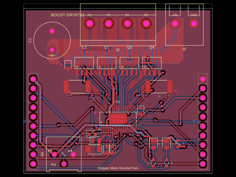 More from this authortscircuit/boostersThis code defines PCB schematics, footprints, and 3D CAD models for various integrated circuits, connectors, sensors, and electronic components used in TI booster packs and modules.
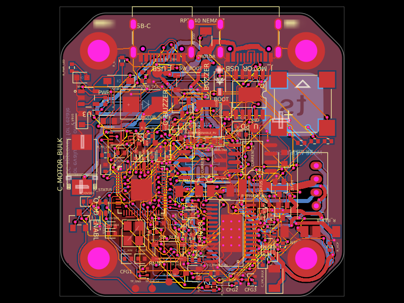 Similar packageimrishabh18/rp2040-motor-controllerA four-layer RP2040-based NEMA17 stepper controller with USB-C power/data, CH224K USB-PD negotiation, DRV8825 dual H-bridge drive, current/temperature telemetry, RGB status LED, buzzer alarm, QSPI flash, and optional AS5600 encoder.
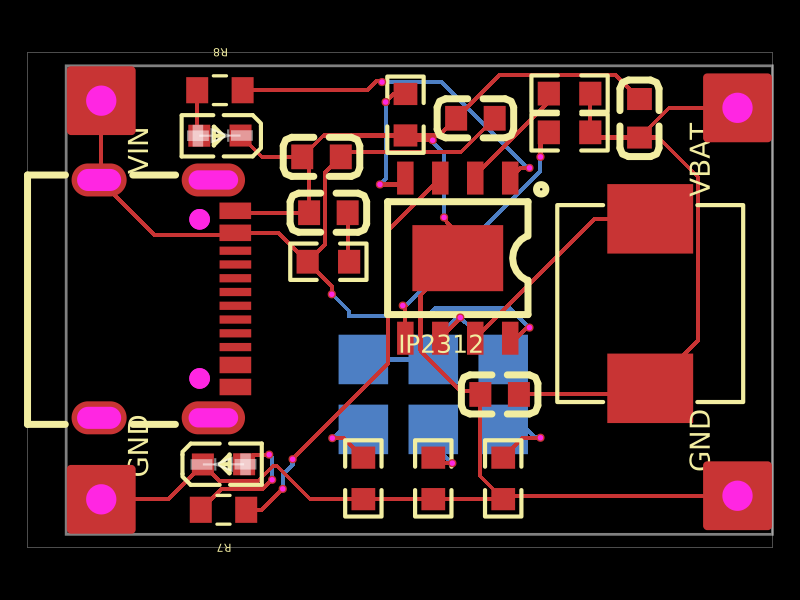 Discover something newkrishnax12/ip2312-fast-charging-moduleThis design implements a compact PCB with a USB-C input port, IP2312 battery charger IC, associated passive components (capacitors, resistors, inductor), output terminals for BAT and GND, and status indicator LEDs, facilitating fast lithium battery charging.