README.md
# ESP32-S3 USB webcam with Arducam M0031

This is a provisional, compact USB 2.0 Full-Speed webcam board. An
ESP32-S3-WROOM-1-N16R8 captures JPEG frames from an external Arducam M0031
OV2640 module over the parallel DVP bus and presents them to a computer as a
USB Video Class (UVC) device. The same USB-C receptacle is used for native USB
bootloader flashing and for the webcam at runtime; there is no USB-to-UART
bridge and no USB Power Delivery controller.

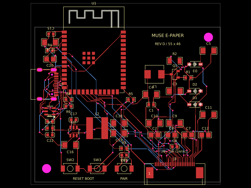
This batch contains the complete schematic, placement, and routed four-layer
PCB. The generated Circuit JSON passes netlist, placement, and short checks with
no reported errors or unrouted connections. It is still an **engineering
reference, not a production release**: connector fit, the selected fabrication
stackup and controlled impedance, power rails, RF clearance, and actual camera
streaming must be validated on hardware before a manufacturing order.

## Architecture

- ESP32-S3-WROOM-1-N16R8, 16 MB flash and 8 MB octal PSRAM, JLCPCB C2913202.
- ESP32 pin-41 EPAD preserves the recommended 3 × 3 segmented thermal-land
  array. Four tented 0.20/0.45 mm grounded through-vias sit in the inter-land
  gaps—not in the solder pads. A solder-mask-covered local top GND island bonds
  all nine lands to those vias and the inner-1 plane while retaining segmented
  solder paste.
- USB-C USB 2.0 device input with independent 5.1 kΩ Rd on CC1 and CC2.
- USB D-/D+ flow through a USBLC6-2SC6 ESD array and 33 Ω series resistors to
  GPIO19/GPIO20. The shell is coupled to logic ground by 1 MΩ in parallel with
  a 4.7 nF, 2 kV capacitor.
- USB VBUS passes through a 750 mA resettable fuse and has a unidirectional
  SMF5.0A TVS before the TLV62569 buck.
- TLV62569 5 V to 3.3 V buck: 2.2 µH, 4.7 µF input, 10 µF output, and a
  453 kΩ / 100 kΩ divider. Its nominal output is
  `0.6 * (1 + 453k / 100k) = 3.318 V`.
- XC6206P282MR provides camera AVDD and DOVDD at 2.8 V.
- SGM2059-ADJ provides camera DVDD. Its 25.5 kΩ / 40.2 kΩ divider gives
  `0.793 * (1 + 25.5k / 40.2k) = 1.296 V` nominal.
- RESET_N has a 10 kΩ pull-up to camera 2.8 V and PWDN has a 10 kΩ pull-down.
  These agree with the inactive states used by the ESP32-S3-EYE camera design;
  neither signal consumes an ESP32 GPIO.
- ESP32 EN uses 10 kΩ / 1 µF power-on reset timing plus a RESET switch. GPIO0
  has a 10 kΩ pull-up plus a BOOT switch.
- UART0 TX/RX/3V3/GND and JTAG GPIO39–GPIO42 plus 3V3/GND are exposed as
  1.2 mm top-side pogo pads.

The provisional PCB is 65.5 mm × 42.5 mm, four layers, and top-side assembly only.
The intended stack strategy is top signals/components, inner-1 uninterrupted
ground reference, inner-2 3.3 V distribution, and bottom signals only where
needed. Bare vias are not assembly items; every machine-assembled part and all
debug pads are explicitly on top.
The USB pair is to be routed on top over inner-1 as a 90 Ω differential pair.
The M0031 DVP bus must be kept short between the ESP32 module and the ZIF. An
all-layer keepout covers the ESP32 module antenna and the area in front of it.
The current camera placement leaves about 3.0 mm of clear first-stage escape
behind the 0.5 mm-pitch signal pads before the two rail HF bypass footprints;
the two bulk capacitors sit outside the signal-pad bank and all camera pull
resistors sit to its left.

The connector uses deterministic manual fanout before phased board routing.
The DNP `CAM_FANOUT_VIAS` footprint provides 16 staggered 0.45/0.20 mm plated
transitions for DVP/control signals, and five DNP rail fanout points handle
AVDD, DVDD, DOVDD, AGND, and DGND. Exact connector-pad-to-fanout segments own
the dense 0.5 mm-pitch escape; the board router starts at the widened fanout
instead of the raw connector pad bank. D2 through D9 and PCLK remain ordered
with ESP32 GPIO9–GPIO14, GPIO21, GPIO47, and GPIO48.

Four 2.7 mm non-plated mounting holes for M2.5 hardware are centered at
`(±30.5, ±19.0) mm`. Each has a 2.5 mm-radius keepout on all four copper
layers. The drill edge is 0.90 mm from the two adjacent board edges. RESET and
BOOT have been moved inward so their imported courtyard/body is approximately
3.0 mm from the right edge. The JTAG 3V3 pad is now at `(30, 11) mm`; its
1.2 mm pad edge is 2.15 mm from the right PCB edge.

The compact outline preserves every electrical pad coordinate from the
short-checked 68 mm × 45 mm routing baseline. Each autorouting phase therefore
replays that proven copper deterministically, while tscircuit regenerates the
board, pours, and DRC results for the smaller outline. A route-endpoint guard
rejects any future component move unless the proven route is deliberately
regenerated and revalidated.

See [`COMPACTNESS_REPORT.md`](./COMPACTNESS_REPORT.md) for the comparison of all
tested outline and placement strategies, including the rejected 48 × 32 mm,
55 × 36 mm, and 58 × 38 mm experiments.

## External camera: the only non-JLC item

Buy one [Arducam M0031 OV2640 24-pin camera module](https://www.arducam.com/arducam-ov2640-camera-module-2mp-mini-ccm-compact-camera-modules-compatible-with-arduino_m0031esp32-esp8266-development-board-with-dvp-24-pin-interface_.html).
The M0031 includes the OV2640 sensor, lens assembly, and its short gold-finger
flex; no sensor or lens soldering is required.

The board-side connector is the JLC-assembled JUSHUO AFC01-S24FCA-00,
JLCPCB C262669: 24
positions, 0.5 mm pitch, 0.3 mm flex thickness, hinged lid, **bottom contact**.
Only this connector has a PCB footprint. The Arducam M0031 is an external,
hand-installed optical module and is not represented as a JLC placement.
Install the camera only with USB power disconnected:

1. Lift the black/brown ZIF latch.
2. Match camera pin 1 to the board's `PIN 1` silkscreen.
3. Slide the M0031 flex fully into the connector with its exposed gold contacts
   facing the PCB: **contacts down**.
4. Close the latch evenly, then inspect that the flex is square and fully
   seated before applying power.

The C262669 connector is intended to replace the module vendor's referenced
Amphenol F32R-1A7H1-11024 mating connector. A physical M0031 sample still has to
prove insertion depth, tail thickness, contact side, pin-1 orientation, and
latch retention before the board can be released.

The camera PCB is an external 21 mm × 12.5 mm mechanical envelope, not a board
component or a JLC placement. The fabrication overlay projects that envelope
from the connector centerline beyond the bottom PCB edge, and a short top-silk
datum marks its 21 mm projected width. The present support strategy is an
enclosure cradle or compliant pad under the external camera PCB, using the four
main-board M2.5 holes to locate the enclosure. No camera mounting-hole pattern
or rigid retainer has been invented: final cradle depth, flex bend, lens-axis
location, and any optional bracket geometry require an actual M0031 sample.
Nothing may obstruct horizontal flex insertion or operation of the top latch.

The [JUSHUO/LCSC mechanical drawing](https://datasheet.lcsc.com/datasheet/pdf/97e3ba016a78286ffa6cfbc591e2beb6.pdf?productCode=C262669)
shows a conventional horizontal SMT connector with a 6.1 mm front-to-back body
and a recommended PCB land pattern; it does not identify an edge overhang. The
placement therefore supports the entire imported footprint. Its imported
courtyard is 0.467 mm inside the bottom PCB edge and the drawn body/silkscreen
is about 0.73 mm inside. The flex still enters horizontally at the unobstructed
bottom edge and the hinged latch remains accessible from the top.

The TLV62569 cell is deliberately clustered around the exact 4.02 mm-class
WPN4020 inductor. The U/L/Cout center span is about 6.75 mm. A 6 mm center span
cannot be achieved without violating the imported inductor and SOT-23
courtyards. VIN-to-HF-Cin, SW-to-L, and L-to-Cout pad-edge gaps are each about
1 mm or less; separate nearby U-ground and Cout-ground vias are reserved for a
short top return plus an inner-1 ground-plane return during the routing batch.

The 1.296 V SGM2059 LDO cell remains the highest current placement-only
routing-difficulty estimate at about 7.5%. That estimate is not a placement
DRC failure, but the cell has deliberately retained access around IN, OUT, FB,
and both ground vias. Its routed copper received a post-route visual review;
OUT-to-divider sensing and the ground return should also be probed during
hardware bring-up.

### Manual ground-via strategy

The routed design keeps deliberate local-return and protection vias. Two
previously optional camera-edge stitching vias, `VIA_GND_STITCH_L` at
`(-26.5, -19.5) mm` and `VIA_GND_STITCH_R` at `(26.5, -19.5) mm`, are
temporarily removed. They did not serve a capacitor or regulator ground and
must not be reintroduced until routed copper makes useful, DRC-clean stitching
locations clear.

The camera-area local-return vias retained are:

- `VIA_GND_CAM_AVDD_BULK`, beside the M0031 2.8 V bulk capacitor ground pad;
- `VIA_GND_CAM_DVDD_BULK`, beside the M0031 1.296 V bulk ground pad;
- `VIA_GND_CAM_2V8_HF` and `VIA_GND_CAM_DVDD_HF`, beside the two HF bypass
  ground pads;
- `VIA_GND_LDO_2V8_IC`, `VIA_GND_LDO_2V8_IN`, and
  `VIA_GND_LDO_2V8_OUT`, for the 2.8 V regulator and its input/output returns;
- `VIA_GND_LDO_1V3_IC`, `VIA_GND_LDO_1V3_IN`, and
  `VIA_GND_LDO_1V3_OUT`, for the 1.296 V regulator and its input/output
  returns.

Two local-return locations were corrected after Gerber-derived short checking:
`VIA_GND_CAM_AVDD_BULK` moved from `(-5, -11.4)` to `(-3.9, -12.6) mm`,
beside rather than above the capacitor ground pad, and
`VIA_GND_LDO_2V8_OUT` moved from `(23.2, -10.05)` to `(22.3, -8.9) mm`,
above the output capacitor ground pad and outside the adjacent SGM2059 FB
courtyard. The autorouter supplies their copper connections; neither uses
via-in-pad.

## Camera GPIO map

| M0031 signal | ESP32-S3 GPIO |
| --- | ---: |
| SDA | 4 |
| SCL | 5 |
| VSYNC | 6 |
| HREF | 7 |
| XCLK | 15 |
| PCLK | 48 |
| D9 | 47 |
| D8 | 21 |
| D7 | 14 |
| D6 | 13 |
| D5 | 12 |
| D4 | 11 |
| D3 | 10 |
| D2 | 9 |

This custom 8-bit mapping uses the module's contiguous lower-edge GPIO9–GPIO14,
GPIO21, GPIO47, and GPIO48 pads to simplify the camera-bus escape. M0031 STROBE,
D1, and D0 are intentionally not connected. The design is specifically for the
N16R8 module. Its S3R8 device does not have the ESP32-S3R16V module variants'
GPIO47/GPIO48 1.8 V-only caveat; substituting an R16V-based module without
reviewing its I/O voltage is not supported.

## Firmware and programming

Start with Espressif's [esp32-camera driver](https://github.com/espressif/esp32-camera)
and the [ESP-IoT-Solution USB webcam device example](https://github.com/espressif/esp-iot-solution/tree/master/examples/usb/device/usb_webcam).
The driver supports ESP32-S3 and OV2640 JPEG output. Use the following
`camera_config_t` pin fields; driver `pin_d0` through `pin_d7` correspond to
sensor D2 through D9 respectively. Configure PWDN and RESET as `-1` because
their inactive levels are fixed by board pull resistors.

```c
.pin_pwdn = -1,
.pin_reset = -1,
.pin_xclk = 15,
.pin_sccb_sda = 4,
.pin_sccb_scl = 5,
.pin_d0 = 9,   // sensor D2
.pin_d1 = 10,  // sensor D3
.pin_d2 = 11,  // sensor D4
.pin_d3 = 12,  // sensor D5
.pin_d4 = 13,  // sensor D6
.pin_d5 = 14,  // sensor D7
.pin_d6 = 21,  // sensor D8
.pin_d7 = 47,  // sensor D9
.pin_vsync = 6,
.pin_href = 7,
.pin_pclk = 48,
```

The first firmware target is **MJPEG, VGA 640 × 480 at 15 fps**. That is an
engineering target, not yet a guaranteed specification. USB Full-Speed is only
12 Mbit/s and a Full-Speed isochronous endpoint can carry roughly 1 MB/s of
payload, so JPEG size and scene complexity matter. QVGA 320 × 240 at 15–30 fps
is the safer fallback. Raw VGA is not realistic on this USB link.

Native USB flashing workflow:

1. Connect the USB-C port to the computer.
2. Hold BOOT, tap RESET, release RESET, then release BOOT. GPIO0 is now sampled
   low and the ESP32-S3 ROM USB bootloader enumerates.
3. Set the ESP-IDF target to ESP32-S3 and flash the selected port with
   `idf.py set-target esp32s3` then `idf.py -p PORT flash monitor`.
4. After reset, the application owns the same USB pins and enumerates as UVC.
   Re-enter ROM download mode with BOOT+RESET if broken firmware stops USB from
   enumerating.

The UART0 pads are a recovery/logging path, but require an external 3.3 V USB
UART adapter and a pogo fixture. Do not feed 5 V logic into the UART pads.

## Critical JLCPCB BOM

Stock numbers below are search snapshots from 2026-08-25 and must be checked
again when ordering. All are JLC-assembly parts; the Arducam M0031 is installed
by hand after assembly.

| Function | Manufacturer part | JLCPCB | Snapshot stock |
| --- | --- | --- | ---: |
| MCU/module | ESP32-S3-WROOM-1-N16R8 | C2913202 | 32,101 |
| Camera ZIF | AFC01-S24FCA-00 | C262669 | 56,931 |
| USB-C receptacle | TYPE-C-31-M-12 | C165948 | 89,797 |
| USB ESD | USBLC6-2SC6 | C2687116 | 150,192 |
| VBUS PTC | BSMD0603-075-6V | C914092 | 96,542 |
| VBUS TVS | SMF5.0A | C193402 | 402,983 |
| 3.3 V buck | TLV62569DBVR | C141836 | 108,275 |
| Buck inductor | WPN4020H2R2MT, 2.2 µH | C98361 | 51,123 |
| Camera 2.8 V LDO | XC6206P282MR | C347374 | 169,833 |
| Camera core LDO | SGM2059-ADJXN5G/TR | C5152783 | 6,203 |
| RESET/BOOT switch | TS-1187A-B-A-B | C318884 | 1,683,297 |
| Shield coupling capacitor | C1206X472K202T, 4.7 nF 2 kV | C106076 | 49,109 |

The SGM2059 is the tightest-stock critical item and should be rechecked first.
The design also carries exact JLC metadata for the feedback, USB, strap, and
decoupling passives in `index.circuit.tsx`.

## Reproducible build

This design is validated with exactly `tscircuit@0.0.2422`, as pinned in
`package.json` and `bun.lock`. Install and build with:

```sh
bun install --frozen-lockfile
bun run build
bun test
```

Do not update tscircuit as part of a manufacturing release without repeating
the complete routing, short, placement, and rendered-copper review. Later
autorouter versions can produce materially different routing from the same
source.

## Primary design references

- [ESP32-S3 series data sheet](https://documentation.espressif.com/esp32_s3_datasheet_en.pdf)
- [ESP32-S3-WROOM-1/1U module data sheet](https://documentation.espressif.com/esp32-s3-wroom-1_wroom-1u_datasheet_en.pdf)
- [ESP32-S3 GPIO matrix and pin restrictions](https://docs.espressif.com/projects/esp-idf/en/stable/esp32s3/api-reference/peripherals/gpio.html)
- [Espressif esp32-camera `camera_config_t`](https://github.com/espressif/esp32-camera/blob/master/driver/include/esp_camera.h)
- [ESP32-S3 hardware schematic checklist](https://docs.espressif.com/projects/esp-hardware-design-guidelines/en/latest/esp32s3/schematic-checklist.html)
- [ESP32-S3 PCB layout guidelines](https://docs.espressif.com/projects/esp-hardware-design-guidelines/en/latest/esp32s3/pcb-layout-design.html)
- [ESP32-S3 native USB boot/console programming](https://docs.espressif.com/projects/esp-idf/en/stable/esp32s3/api-guides/usb-otg-console.html)
- [TI TLV62569 data sheet](https://www.ti.com/lit/ds/symlink/tlv62569.pdf)
- [SGMICRO SGM2059 data sheet](https://www.sg-micro.com/rect/assets/c90e4805-a9a9-4001-be72-fb96737d867e/SGM2059.pdf)
- [Torex XC6206 data sheet](https://product.torexsemi.com/system/files/series/xc6206.pdf)
- [ST USBLC6-2 data sheet](https://www.st.com/resource/en/datasheet/usblc6-2.pdf)
- [JLCPCB C262669 connector listing](https://jlcpcb.com/partdetail/C262669)
- [JUSHUO AFC01 series mechanical drawing and recommended PCB pattern](https://datasheet.lcsc.com/datasheet/pdf/97e3ba016a78286ffa6cfbc591e2beb6.pdf?productCode=C262669)

## Outstanding release checks

- Buy an M0031 sample and validate the ZIF mating geometry and complete pinout
  with continuity before connecting the sensor.
- Measure 3.3 V, 2.8 V, and 1.296 V unloaded and with a streaming camera.
- Confirm USB inrush/current descriptors and PTC drop under worst-case Wi-Fi +
  camera load, even if Wi-Fi is not used by the default webcam firmware.
- Choose the actual JLC four-layer stackup and confirm that the routed USB pair
  geometry produces 90 Ω differential impedance before fabrication.
- Review PCLK/XCLK/data and the inner-1 return plane against the chosen stackup;
  repeat DRC, shorts, and trace-length checks after any routing edit.
- Probe and thermally inspect the routed 1.296 V LDO cell during bring-up.
- Validate UVC descriptors and MJPEG frame size on Windows, macOS, and Linux;
  characterize VGA15 and the QVGA fallback over scene complexity and lighting.
- Verify RF antenna clearance with the enclosure and camera flex installed.
- Inspect the high-resolution PCB, schematic, and 3D renders before generating
  manufacturing files.