0hmX/esp32-s3-usb-webcam-ov2640
This code defines and integrates a variety of surface-mount, through-hole, and connector hardware components (including microcontrollers, regulators, resistors, capacitors, and connectors) into a PCB design framework, enabling schematic symbol creation, footprint definition, and automated routing within an electronic circuit layout.
- Version
- 1.0.7
- License
- unset
- Stars
- 0
index.circuit.tsx
PCB
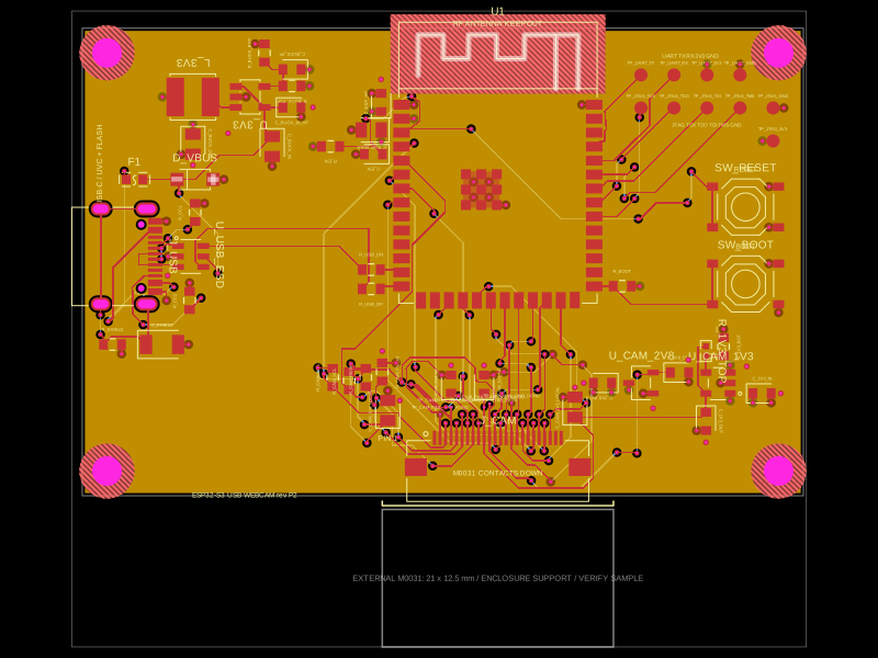
Schematic

import { AFC01_S24FCA_00 } from "./imports/AFC01_S24FCA_00"
import { Fragment } from "react"
import { BSMD0603_075_6V } from "./imports/BSMD0603_075_6V"
import { ESP32_S3_WROOM_1_N16R8 } from "./imports/ESP32_S3_WROOM_1_N16R8"
import { FRC0402F2552TS } from "./imports/FRC0402F2552TS"
import { SGM2059_ADJXN5G_TR } from "./imports/SGM2059_ADJXN5G_TR"
import { SMF5_0A } from "./imports/SMF5_0A"
import { TLV62569DBVR } from "./imports/TLV62569DBVR"
import { TS_1187A_B_A_B } from "./imports/TS_1187A_B_A_B"
import { TYPE_C_31_M_12 } from "./imports/TYPE_C_31_M_12"
import { USBLC6_2SC6 } from "./imports/USBLC6_2SC6"
import { WPN4020H2R2MT } from "./imports/WPN4020H2R2MT"
import { XC6206P282MR } from "./imports/XC6206P282MR"
import { createProvenRouteAutorouter } from "./src/proven-route-autorouter"
import { BOARD_ROUTING_PHASES } from "./src/routing-phases"

const USB = "USB_INPUT"
const POWER = "POWER_3V3"
const ESP = "ESP32_S3"
const ESP_PCB_X = 5
const ESP_PCB_Y = 5.25
const CAMERA_POWER = "CAMERA_POWER"
const CAMERA = "ARDUCAM_M0031_DVP"
const CONTROL = "BOOT_RESET"
const DEBUG = "DEBUG_PADS"
const SYSTEM_SHEET = "SYSTEM_USB"
const CAMERA_SHEET = "CAMERA_INTERFACE"

const schematicXOffset: Record<string, number> = {
  [USB]: 0,
  [POWER]: 0,
  [ESP]: 0,
  [CAMERA_POWER]: 0,
  [CAMERA]: 0,
  [CONTROL]: 0,
  [DEBUG]: 0,
}

const schematicYOffset: Record<string, number> = {
  [USB]: 0,
  [POWER]: 0,
  [ESP]: 0,
  [CAMERA_POWER]: 0,
  [CAMERA]: 0,
  [CONTROL]: 0,
  [DEBUG]: 0,
}

const schematicSheetForSection: Record<string, string> = {
  [USB]: SYSTEM_SHEET,
  [POWER]: SYSTEM_SHEET,
  [ESP]: SYSTEM_SHEET,
  [CAMERA_POWER]: CAMERA_SHEET,
  [CAMERA]: CAMERA_SHEET,
  [CONTROL]: SYSTEM_SHEET,
  [DEBUG]: SYSTEM_SHEET,
}

const schematicScaleForSection: Record<string, { x: number; y: number }> = {
  // Keep each functional block compact enough to scan without long runs of
  // empty page, while leaving the large imported symbols room for pin labels.
  [USB]: { x: 0.9, y: 0.9 },
  [POWER]: { x: 0.9, y: 0.9 },
  [ESP]: { x: 0.94, y: 0.92 },
  [CAMERA_POWER]: { x: 0.9, y: 0.9 },
  [CAMERA]: { x: 0.9, y: 0.9 },
  [CONTROL]: { x: 0.9, y: 0.9 },
  [DEBUG]: { x: 0.7, y: 0.7 },
}

const scaledSchX = (section: string, x: number) =>
  x * schematicScaleForSection[section].x

const scaledSchY = (section: string, y: number) =>
  y * schematicScaleForSection[section].y

const resistorParts = {
  r33: { value: "33", lcsc: "C23140", mpn: "0603WAF330JT5E", footprint: "0603" },
  r4k7: { value: "4.7k", lcsc: "C23162", mpn: "0603WAF4701T5E", footprint: "0603" },
  r5k1: { value: "5.1k", lcsc: "C23186", mpn: "0603WAF5101T5E", footprint: "0603" },
  r10k: { value: "10k", lcsc: "C25804", mpn: "0603WAF1002T5E", footprint: "0603" },
  r40k2: { value: "40.2k", lcsc: "C2933218", mpn: "FRC0603F4022TS", footprint: "0603" },
  r100k: { value: "100k", lcsc: "C25803", mpn: "0603WAF1003T5E", footprint: "0603" },
  r453k: { value: "453k", lcsc: "C3013202", mpn: "FRC0603F4533TS", footprint: "0603" },
  r1m: { value: "1M", lcsc: "C22935", mpn: "0603WAF1004T5E", footprint: "0603" },
} as const

const capacitorParts = {
  c6p8: { value: "6.8pF", lcsc: "C1679", mpn: "0603CG6R8C500NT", footprint: "0603" },
  c4n7_2kV: { value: "4.7nF", lcsc: "C106076", mpn: "C1206X472K202T", footprint: "1206" },
  c100n: { value: "100nF", lcsc: "C14663", mpn: "CC0603KRX7R9BB104", footprint: "0603" },
  c1u: { value: "1uF", lcsc: "C113807", mpn: "CC0603KRX7R6BB105", footprint: "0603" },
  c4u7: { value: "4.7uF", lcsc: "C2857993", mpn: "0805B475K100NT", footprint: "0805" },
  c10u: { value: "10uF", lcsc: "C86038", mpn: "GRM21BR71A106KE51L", footprint: "0805" },
} as const

type ResistorKey = keyof typeof resistorParts
type CapacitorKey = keyof typeof capacitorParts
type PassiveConfig<K extends string> = {
  name: string
  displayName: string
  part: K
  a: string
  b: string
  pcbX: number
  pcbY: number
  pcbRotation: number
  layer: "top"
  schX: number
  schY: number
  schOrientation?: "horizontal" | "vertical"
  schSectionName: string
}

const resistors: PassiveConfig<ResistorKey>[] = [
  { name: "R_CC1", displayName: "USB-C CC1 Rd", part: "r5k1", a: "USB_CC1", b: "GND", pcbX: -22.5, pcbY: 4.5, pcbRotation: 90, layer: "top", schX: -14, schY: 3, schOrientation: "vertical", schSectionName: USB },
  { name: "R_CC2", displayName: "USB-C CC2 Rd", part: "r5k1", a: "USB_CC2", b: "GND", pcbX: -23, pcbY: -3.5, pcbRotation: 90, layer: "top", schX: -11.5, schY: 3, schOrientation: "vertical", schSectionName: USB },
  { name: "R_USB_DN", displayName: "USB D- series / source termination", part: "r33", a: "USB_DN_ESD", b: "USB_DN_MCU", pcbX: -6.5, pcbY: -0.7, pcbRotation: 0, layer: "top", schX: -3.6, schY: 5.8, schSectionName: USB },
  { name: "R_USB_DP", displayName: "USB D+ series / source termination", part: "r33", a: "USB_DP_ESD", b: "USB_DP_MCU", pcbX: -6.5, pcbY: -2.45, pcbRotation: 0, layer: "top", schX: -4.5, schY: 4.5, schSectionName: USB },
  { name: "R_SHIELD", displayName: "USB shield bleed", part: "r1m", a: "USB_SHIELD", b: "GND", pcbX: -30, pcbY: -7.5, pcbRotation: 0, layer: "top", schX: -8.5, schY: 3.5, schOrientation: "vertical", schSectionName: USB },
  { name: "R_BUCK_TOP", displayName: "3.3V feedback upper", part: "r453k", a: "VCC3V3", b: "BUCK_FB", pcbX: -13.7, pcbY: 16, pcbRotation: 180, layer: "top", schX: 2, schY: 8.5, schSectionName: POWER },
  { name: "R_BUCK_BOT", displayName: "3.3V feedback lower", part: "r100k", a: "BUCK_FB", b: "GND", pcbX: -16.2, pcbY: 19, pcbRotation: 90, layer: "top", schX: 0, schY: 6, schSectionName: POWER },
  { name: "R_1V3_BOT", displayName: "1.296V feedback lower", part: "r40k2", a: "CAM_1V3_FB", b: "GND", pcbX: 25.5, pcbY: -7.7, pcbRotation: 90, layer: "top", schX: -7.5, schY: -2.5, schSectionName: CAMERA_POWER },
  { name: "R_CAM_SDA", displayName: "SCCB SDA pull-up to 2V8", part: "r4k7", a: "CAM_SDA", b: "CAM_2V8", pcbX: -10, pcbY: -10.5, pcbRotation: 90, layer: "top", schX: -10, schY: -2, schOrientation: "vertical", schSectionName: CAMERA },
  { name: "R_CAM_SCL", displayName: "SCCB SCL pull-up to 2V8", part: "r4k7", a: "CAM_SCL", b: "CAM_2V8", pcbX: -8.5, pcbY: -10.8, pcbRotation: 90, layer: "top", schX: -4.5, schY: -2, schOrientation: "vertical", schSectionName: CAMERA },
  { name: "R_CAM_RESET", displayName: "OV2640 RESET_N pull-up", part: "r10k", a: "CAM_RESET_N", b: "CAM_2V8", pcbX: -7, pcbY: -10.5, pcbRotation: 90, layer: "top", schX: 5.2, schY: -6, schOrientation: "vertical", schSectionName: CAMERA },
  { name: "R_CAM_PWDN", displayName: "OV2640 PWDN pull-down", part: "r10k", a: "CAM_PWDN", b: "GND", pcbX: -5.5, pcbY: -10, pcbRotation: 90, layer: "top", schX: 1.5, schY: -6, schOrientation: "vertical", schSectionName: CAMERA },
  { name: "R_EN", displayName: "EN pull-up", part: "r10k", a: "ESP_EN", b: "VCC3V3", pcbX: -10.2, pcbY: 10.5, pcbRotation: 180, layer: "top", schX: 8, schY: 8, schOrientation: "vertical", schSectionName: CONTROL },
  { name: "R_BOOT", displayName: "GPIO0 boot pull-up", part: "r10k", a: "ESP_GPIO0", b: "VCC3V3", pcbX: 16.3, pcbY: -2.2, pcbRotation: 0, layer: "top", schX: 8, schY: 3, schOrientation: "vertical", schSectionName: CONTROL },
]

const capacitors: PassiveConfig<CapacitorKey>[] = [
  { name: "C_SHIELD", displayName: "USB shield HF coupling 2kV", part: "c4n7_2kV", a: "USB_SHIELD", b: "GND", pcbX: -25.5, pcbY: -7.5, pcbRotation: 0, layer: "top", schX: -5, schY: 3, schOrientation: "vertical", schSectionName: USB },
  { name: "C_BUCK_IN", displayName: "Buck input bulk", part: "c4u7", a: "VBUS5V", b: "GND", pcbX: -15.5, pcbY: 10.5, pcbRotation: 270, layer: "top", schX: -6.5, schY: 7.5, schOrientation: "vertical", schSectionName: POWER },
  { name: "C_BUCK_IN_HF", displayName: "Buck VIN bypass", part: "c100n", a: "VBUS5V", b: "GND", pcbX: -13.7, pcbY: 14.05, pcbRotation: 0, layer: "top", schX: -3, schY: 7.5, schOrientation: "vertical", schSectionName: POWER },
  { name: "C_BUCK_OUT", displayName: "Buck output filter", part: "c10u", a: "VCC3V3", b: "GND", pcbX: -22.7, pcbY: 10.7, pcbRotation: 270, layer: "top", schX: -1.5, schY: 7.5, schOrientation: "vertical", schSectionName: POWER },
  { name: "C_BUCK_FF", displayName: "Buck feed-forward", part: "c6p8", a: "VCC3V3", b: "BUCK_FB", pcbX: -13.7, pcbY: 17.5, pcbRotation: 180, layer: "top", schX: 0, schY: 4, schOrientation: "vertical", schSectionName: POWER },
  { name: "C_ESP_BULK", displayName: "ESP32 local bulk", part: "c10u", a: "VCC3V3", b: "GND", pcbX: -6.5, pcbY: 12, pcbRotation: 180, layer: "top", schX: 1.5, schY: 2, schOrientation: "vertical", schSectionName: ESP },
  { name: "C_ESP_HF", displayName: "ESP32 3V3 bypass", part: "c100n", a: "VCC3V3", b: "GND", pcbX: -5.6, pcbY: 14.5, pcbRotation: 90, layer: "top", schX: 4.5, schY: 2, schOrientation: "vertical", schSectionName: ESP },
  { name: "C_2V8_IN", displayName: "2V8 LDO input", part: "c1u", a: "VCC3V3", b: "GND", pcbX: 14.5, pcbY: -11, pcbRotation: 180, layer: "top", schX: -13, schY: 4, schOrientation: "vertical", schSectionName: CAMERA_POWER },
  { name: "C_2V8_OUT", displayName: "2V8 LDO output", part: "c1u", a: "CAM_2V8", b: "GND", pcbX: 21.5, pcbY: -10.05, pcbRotation: 0, layer: "top", schX: -9, schY: 4, schOrientation: "vertical", schSectionName: CAMERA_POWER },
  { name: "C_1V3_IN", displayName: "1V296 LDO input", part: "c1u", a: "VCC3V3", b: "GND", pcbX: 29, pcbY: -11.95, pcbRotation: 0, layer: "top", schX: -13, schY: -2.5, schOrientation: "vertical", schSectionName: CAMERA_POWER },
  { name: "C_1V3_OUT", displayName: "1V296 LDO output", part: "c1u", a: "CAM_1V3", b: "GND", pcbX: 23.9, pcbY: -14.5, pcbRotation: 270, layer: "top", schX: -9, schY: -4, schOrientation: "vertical", schSectionName: CAMERA_POWER },
  { name: "C_CAM_2V8_LOCAL", displayName: "M0031 AVDD 2V8 local bulk", part: "c4u7", a: "CAM_2V8", b: "GND", pcbX: -5, pcbY: -13.5, pcbRotation: 90, layer: "top", schX: 5, schY: 5, schOrientation: "vertical", schSectionName: CAMERA },
  { name: "C_CAM_2V8_HF", displayName: "M0031 AVDD/DOVDD 2V8 bypass", part: "c100n", a: "CAM_2V8", b: "GND", pcbX: 0.75, pcbY: -11.1, pcbRotation: 90, layer: "top", schX: 10, schY: 5, schOrientation: "vertical", schSectionName: CAMERA },
  { name: "C_CAM_1V3_LOCAL", displayName: "M0031 DVDD 1V296 local bulk", part: "c4u7", a: "CAM_1V3", b: "GND", pcbX: 12, pcbY: -13.2, pcbRotation: 90, layer: "top", schX: 5, schY: -4, schOrientation: "vertical", schSectionName: CAMERA },
  { name: "C_CAM_1V3_HF", displayName: "M0031 DVDD 1V296 bypass", part: "c100n", a: "CAM_1V3", b: "GND", pcbX: 3.75, pcbY: -11.1, pcbRotation: 90, layer: "top", schX: 9, schY: -4, schOrientation: "vertical", schSectionName: CAMERA },
  { name: "C_EN", displayName: "EN power-on delay", part: "c1u", a: "ESP_EN", b: "GND", pcbX: -6.3, pcbY: 9.8, pcbRotation: 180, layer: "top", schX: 12, schY: 8, schOrientation: "vertical", schSectionName: CONTROL },
]

const debugPads = [
  ["TP_UART_TX", "UART0_TX", 18, 17, 2, -3],
  ["TP_UART_RX", "UART0_RX", 21, 17, 5, -3],
  ["TP_UART_3V3", "VCC3V3", 24, 17, 8, -3],
  ["TP_UART_GND", "GND", 27, 17, 11, -3],
  ["TP_JTAG_TCK", "JTAG_TCK", 18, 14, 0, -6],
  ["TP_JTAG_TDO", "JTAG_TDO", 21, 14, 2.7, -6],
  ["TP_JTAG_TDI", "JTAG_TDI", 24, 14, 5.4, -6],
  ["TP_JTAG_TMS", "JTAG_TMS", 27, 14, 8.1, -6],
  ["TP_JTAG_GND", "GND", 30, 14, 10.8, -6],
  ["TP_JTAG_3V3", "VCC3V3", 30, 11, 13.5, -6],
] as const

// Two staggered rows of through-hole breakout points provide the deliberate
// layer transition outside the 0.5 mm FPC pad row. The connector-to-breakout
// segment is exact manual copper; only the roomy breakout-to-destination run
// is handed to the board autorouter.
const cameraFanoutRoutes = [
  { pin: "SDA", net: "CAM_SDA", x: 0.2502, row: 0, destination: "IO4", branchDestination: ".R_CAM_SDA > .pin1", phaseIndex: 3 },
  { pin: "SCL", net: "CAM_SCL", x: 1.2502, row: 0, destination: "IO5", branchDestination: ".R_CAM_SCL > .pin1", phaseIndex: 3 },
  { pin: "RESET_N", net: "CAM_RESET_N", x: 1.7501, row: 1, destination: null, branchDestination: ".R_CAM_RESET > .pin1", phaseIndex: 3 },
  { pin: "VSYNC", net: "CAM_VSYNC", x: 2.2502, row: 0, destination: "IO6", branchDestination: null, phaseIndex: 1 },
  { pin: "PWDN", net: "CAM_PWDN", x: 2.7501, row: 1, destination: null, branchDestination: ".R_CAM_PWDN > .pin1", phaseIndex: 3 },
  { pin: "HREF", net: "CAM_HREF", x: 3.2502, row: 0, destination: "IO7", branchDestination: null, phaseIndex: 1 },
  { pin: "D9", net: "CAM_D9", x: 4.7501, row: 1, destination: "IO47", branchDestination: null, phaseIndex: 1 },
  { pin: "XCLK", net: "CAM_XCLK", x: 5.2502, row: 0, destination: "IO15", branchDestination: null, phaseIndex: 1 },
  { pin: "D8", net: "CAM_D8", x: 5.7501, row: 1, destination: "IO21", branchDestination: null, phaseIndex: 1 },
  { pin: "D7", net: "CAM_D7", x: 6.7501, row: 1, destination: "IO14", branchDestination: null, phaseIndex: 1 },
  { pin: "PCLK", net: "CAM_PCLK", x: 7.2502, row: 0, destination: "IO48", branchDestination: null, phaseIndex: 1 },
  { pin: "D6", net: "CAM_D6", x: 7.7501, row: 1, destination: "IO13", branchDestination: null, phaseIndex: 1 },
  { pin: "D2", net: "CAM_D2", x: 8.2502, row: 0, destination: "IO9", branchDestination: null, phaseIndex: 1 },
  { pin: "D5", net: "CAM_D5", x: 8.7501, row: 1, destination: "IO12", branchDestination: null, phaseIndex: 1 },
  { pin: "D3", net: "CAM_D3", x: 9.2502, row: 0, destination: "IO10", branchDestination: null, phaseIndex: 1 },
  { pin: "D4", net: "CAM_D4", x: 9.7501, row: 1, destination: "IO11", branchDestination: null, phaseIndex: 1 },
] as const

const cameraRailFanoutRoutes = [
  { connectorPin: "AGND", fanoutPin: "GND_AGND", net: "GND", x: -0.25, y: -13.85 },
  { connectorPin: "AVDD_2V8", fanoutPin: "CAM_2V8_AVDD", net: "CAM_2V8", x: 0.75, y: -13.2 },
  { connectorPin: "DVDD_1V3", fanoutPin: "CAM_1V3_DVDD", net: "CAM_1V3", x: 3.75, y: -13.2 },
  { connectorPin: "DOVDD_2V8", fanoutPin: "CAM_2V8_DOVDD", net: "CAM_2V8", x: 4.25, y: -12.9 },
  { connectorPin: "DGND", fanoutPin: "GND_DGND", net: "GND", x: 6.25, y: -12.8 },
] as const

const cameraFanoutPinLabels = Object.fromEntries(
  cameraFanoutRoutes.map(({ pin }, index) => [`pin${index + 1}`, pin]),
)

export default function Esp32S3UsbWebcamOv2640() {
  return (
    <board
      name="ESP32_S3_USB_WEBCAM_OV2640"
      title="ESP32-S3 USB webcam / Arducam M0031"
      width="65.5mm"
      height="42.5mm"
      layers={4}
      autorouter={{
        local: true,
        groupMode: "subcircuit",
        algorithmFn: createProvenRouteAutorouter,
      }}
      schTraceAutoLabelEnabled
      minTraceWidth="0.15mm"
      minViaHoleDiameter="0.2mm"
      minViaPadDiameter="0.45mm"
      minBoardEdgeClearance="0.25mm"
    >
      <schematicsheet
        name={SYSTEM_SHEET}
        displayName="SYSTEM + USB"
        sheetIndex={0}
      >
        <schematicsection name={USB} displayName="USB-C DEVICE INPUT + PROTECTION" />
        <schematicsection name={POWER} displayName="5 V TO 3.3 V BUCK" />
        <schematicsection name={ESP} displayName="ESP32-S3-WROOM-1-N16R8" />
        <schematicsection name={CONTROL} displayName="RESET + BOOT STRAPS" />
        <schematicsection name={DEBUG} displayName="UART0 + OPTIONAL JTAG PADS" />
        <schematictext
          text="USB 2.0 FULL-SPEED: VERIFY 90 OHM DIFFERENTIAL IMPEDANCE WITH FINAL STACKUP"
          schX={0}
          schY={-9.7}
          fontSize={0.22}
          color="#555555"
        />
      </schematicsheet>
      <schematicsheet
        name={CAMERA_SHEET}
        displayName="CAMERA INTERFACE"
        sheetIndex={1}
      >
        <schematicsection name={CAMERA_POWER} displayName="CAMERA 2.8 V + 1.296 V RAILS" />
        <schematicsection name={CAMERA} displayName="ARDUCAM M0031 / OV2640 DVP" />
        <schematictext
          text="NC BY DESIGN: STROBE, D1, D0  |  RESET_N=PULLED HIGH  |  PWDN=PULLED LOW"
          schX={0}
          schY={9.5}
          fontSize={0.22}
          color="#555555"
        />
      </schematicsheet>

      {/* L2 is the continuous high-speed reference plane. L3 distributes 3V3.
          The all-layer keepout covers the PCB antenna and space in front. */}
      <copperpour name="GND_PLANE_INNER1" layer="inner1" connectsTo="net.GND" unbroken clearance="0.2mm" boardEdgeMargin="0.25mm" />
      <copperpour name="V3V3_PLANE_INNER2" layer="inner2" connectsTo="net.VCC3V3" unbroken clearance="0.2mm" boardEdgeMargin="0.25mm" />
      <copperpour
        name="GND_POUR_ESP_EPAD_TOP"
        layer="top"
        connectsTo="net.GND"
        coveredWithSolderMask
        useThermalReliefs={false}
        clearance="0.2mm"
        outline={[
          { x: 1.6498289, y: 4.7248296 },
          { x: 5.3499231, y: 4.7248296 },
          { x: 5.3499231, y: 8.4249238 },
          { x: 1.6498289, y: 8.4249238 },
        ]}
      />
      <keepout shape="rect" layers={["top", "inner1", "inner2", "bottom"]} pcbX={5} pcbY={18.9} width="19.5mm" height="7.2mm" />

      {/* Four M2.5 mounting provisions. The 2.7 mm drills are NPTH, while the
          2.5 mm all-copper keepout radius gives each hole 1.15 mm of annular
          mechanical clearance. Hole edges remain 2.15 mm from both PCB edges. */}
      <hole name="H1" pcbX={-30.5} pcbY={19} diameter="2.7mm" />
      <hole name="H2" pcbX={30.5} pcbY={19} diameter="2.7mm" />
      <hole name="H3" pcbX={-30.5} pcbY={-19} diameter="2.7mm" />
      <hole name="H4" pcbX={30.5} pcbY={-19} diameter="2.7mm" />
      <keepout shape="circle" layers={["top", "inner1", "inner2", "bottom"]} radius="2.5mm" pcbX={-30.5} pcbY={19} />
      <keepout shape="circle" layers={["top", "inner1", "inner2", "bottom"]} radius="2.5mm" pcbX={30.5} pcbY={19} />
      <keepout shape="circle" layers={["top", "inner1", "inner2", "bottom"]} radius="2.5mm" pcbX={-30.5} pcbY={-19} />
      <keepout shape="circle" layers={["top", "inner1", "inner2", "bottom"]} radius="2.5mm" pcbX={30.5} pcbY={-19} />

      <TYPE_C_31_M_12
        name="J_USB"
        displayName="USB-C USB2 DEVICE"
        layer="top"
        pcbX={-28.3}
        pcbY={0.5}
        pcbRotation={-90}
        schX={scaledSchX(USB, -13)}
        schY={scaledSchY(USB, 6)}
        schSheetName={SYSTEM_SHEET}
        schSectionName={USB}
        connections={{ EH1: "net.USB_SHIELD", EH2: "net.USB_SHIELD", EH3: "net.USB_SHIELD", EH4: "net.USB_SHIELD", CC1: "net.USB_CC1", CC2: "net.USB_CC2", DN1: "net.USB_DN_CONN", DN2: "net.USB_DN_CONN", DP1: "net.USB_DP_CONN", DP2: "net.USB_DP_CONN", GND1: "net.GND", GND2: "net.GND", VBUS1: "net.USB_VBUS_RAW", VBUS2: "net.USB_VBUS_RAW" }}
      />
      {/* ST USBLC6-2 flow-through topology: 1->6 is D-, 3->4 is D+. */}
      <USBLC6_2SC6
        name="U_USB_ESD"
        displayName="USBLC6-2SC6 USB ESD"
        layer="top"
        pcbX={-22.9}
        pcbY={0.5}
        pcbRotation={-90}
        schX={scaledSchX(USB, -8.4)}
        schY={scaledSchY(USB, 6)}
        schSheetName={SYSTEM_SHEET}
        schSectionName={USB}
        connections={{ pin1: "net.USB_DN_CONN", GND: "net.GND", pin3: "net.USB_DP_CONN", pin4: "net.USB_DP_ESD", VBUS: "net.VBUS5V", pin6: "net.USB_DN_ESD" }}
      />
      <BSMD0603_075_6V name="F1" displayName="USB VBUS 750mA PTC" layer="top" pcbX={-28} pcbY={7.5} pcbRotation={0} schX={scaledSchX(USB, -12)} schY={scaledSchY(USB, 9)} schSheetName={SYSTEM_SHEET} schSectionName={USB} connections={{ pin1: "net.USB_VBUS_RAW", pin2: "net.VBUS5V" }} />
      <SMF5_0A name="D_VBUS" displayName="5V VBUS TVS" layer="top" pcbX={-22.5} pcbY={7.5} pcbRotation={0} schX={scaledSchX(USB, -9)} schY={scaledSchY(USB, 9)} schWidth={1.2} schSheetName={SYSTEM_SHEET} schSectionName={USB} connections={{ C: "net.VBUS5V", A: "net.GND" }} />

      {/* TI recommended stable 2.2uH/10uF network. 0.6*(1+453k/100k)
          is 3.318V nominal. */}
      <TLV62569DBVR name="U_3V3" displayName="TLV62569 3V3 BUCK" layer="top" pcbX={-17.5} pcbY={15} pcbRotation={180} schX={scaledSchX(POWER, -5.5)} schY={scaledSchY(POWER, 9)} schHeight={0.6} schSheetName={SYSTEM_SHEET} schSectionName={POWER} connections={{ EN: "net.VBUS5V", GND: "net.GND", SW: "net.BUCK_SW", VIN: "net.VBUS5V", FB: "net.BUCK_FB" }} />
      <WPN4020H2R2MT name="L_3V3" layer="top" pcbX={-22.7} pcbY={15} pcbRotation={180} schX={scaledSchX(POWER, -1.5)} schY={scaledSchY(POWER, 9)} schSheetName={SYSTEM_SHEET} schSectionName={POWER} connections={{ pin1: "net.BUCK_SW", pin2: "net.VCC3V3" }} />

      <ESP32_S3_WROOM_1_N16R8
        name="U1"
        displayName="ESP32-S3-WROOM-1-N16R8"
        layer="top"
        pcbX={ESP_PCB_X}
        pcbY={ESP_PCB_Y}
        pcbRotation={0}
        schX={scaledSchX(ESP, 5)}
        schY={scaledSchY(ESP, 6)}
        schHeight={4.2}
        schSheetName={SYSTEM_SHEET}
        schSectionName={ESP}
        connections={{ GND1: "net.GND", GND2: "net.GND", GND3: "net.GND", "3V3": "net.VCC3V3", EN: "net.ESP_EN", IO0: "net.ESP_GPIO0", IO19: "net.USB_DN_MCU", IO20: "net.USB_DP_MCU", IO39: "net.JTAG_TCK", IO40: "net.JTAG_TDO", IO41: "net.JTAG_TDI", IO42: "net.JTAG_TMS", RXD0: "net.UART0_RX", TXD0: "net.UART0_TX" }}
      />

      {/* Four through-vias occupy only the 0.5 mm gaps between the ESP32
          pin-41 lands. Their drill centers and annuli remain outside every
          solder pad; fabrication should tent them from both sides. */}
      <via name="VIA_GND_ESP_EPAD_NW" connectsTo="net.GND" fromLayer="top" toLayer="bottom" pcbX={2.799852} pcbY={5.8748527} outerDiameter="0.45mm" holeDiameter="0.2mm" />
      <via name="VIA_GND_ESP_EPAD_NE" connectsTo="net.GND" fromLayer="top" toLayer="bottom" pcbX={4.1999} pcbY={5.8748527} outerDiameter="0.45mm" holeDiameter="0.2mm" />
      <via name="VIA_GND_ESP_EPAD_SW" connectsTo="net.GND" fromLayer="top" toLayer="bottom" pcbX={2.799852} pcbY={7.2749007} outerDiameter="0.45mm" holeDiameter="0.2mm" />
      <via name="VIA_GND_ESP_EPAD_SE" connectsTo="net.GND" fromLayer="top" toLayer="bottom" pcbX={4.1999} pcbY={7.2749007} outerDiameter="0.45mm" holeDiameter="0.2mm" />

      <XC6206P282MR name="U_CAM_2V8" displayName="CAMERA AVDD/DOVDD 2V8" layer="top" pcbX={18} pcbY={-11} pcbRotation={0} schX={scaledSchX(CAMERA_POWER, -11)} schY={scaledSchY(CAMERA_POWER, 6)} schHeight={0.4} schSheetName={CAMERA_SHEET} schSectionName={CAMERA_POWER} connections={{ VSS: "net.GND", VOUT: "net.CAM_2V8", VIN: "net.VCC3V3" }} />
      {/* SGM2059: 0.793*(1+25.5k/40.2k) = 1.296V nominal. */}
      <SGM2059_ADJXN5G_TR name="U_CAM_1V3" displayName="CAMERA DVDD 1V296" layer="top" pcbX={25} pcbY={-11} pcbRotation={0} schX={scaledSchX(CAMERA_POWER, -11)} schY={scaledSchY(CAMERA_POWER, 0)} schHeight={0.6} schSheetName={CAMERA_SHEET} schSectionName={CAMERA_POWER} connections={{ IN: "net.VCC3V3", GND: "net.GND", EN: "net.VCC3V3", FB: "net.CAM_1V3_FB", OUT: "net.CAM_1V3" }} />
      <FRC0402F2552TS name="R_1V3_TOP" displayName="1.296V feedback upper" layer="top" pcbX={23.9} pcbY={-8.1} pcbRotation={270} schX={scaledSchX(CAMERA_POWER, -8.5)} schY={scaledSchY(CAMERA_POWER, -1)} schSheetName={CAMERA_SHEET} schSectionName={CAMERA_POWER} connections={{ pin1: "net.CAM_1V3", pin2: "net.CAM_1V3_FB" }} />

      {/* Espressif EN RC plus default-high GPIO0 boot strap. Each switch has
          both duplicated physical pads explicitly tied to the same net. */}
      <TS_1187A_B_A_B name="SW_RESET" displayName="RESET" layer="top" pcbX={27.5} pcbY={5} pcbRotation={0} schX={scaledSchX(CONTROL, 11)} schY={scaledSchY(CONTROL, 6.5)} schSheetName={SYSTEM_SHEET} schSectionName={CONTROL} connections={{ A: "net.ESP_EN", C: "net.ESP_EN", B: "net.GND", D: "net.GND" }} />
      <TS_1187A_B_A_B name="SW_BOOT" displayName="BOOT / GPIO0" layer="top" pcbX={27.5} pcbY={-2} pcbRotation={0} schX={scaledSchX(CONTROL, 11)} schY={scaledSchY(CONTROL, 3.55)} schSheetName={SYSTEM_SHEET} schSectionName={CONTROL} connections={{ A: "net.ESP_GPIO0", C: "net.ESP_GPIO0", B: "net.GND", D: "net.GND" }} />

      {resistors.map(({ part, a, b, schX, schY, ...props }) => {
        const p = resistorParts[part]
        return <resistor key={props.name} resistance={p.value} footprint={p.footprint} supplierPartNumbers={{ jlcpcb: [p.lcsc] }} manufacturerPartNumber={p.mpn} connections={{ pin1: `net.${a}`, pin2: `net.${b}` }} schX={scaledSchX(props.schSectionName, schX + schematicXOffset[props.schSectionName])} schY={scaledSchY(props.schSectionName, schY + schematicYOffset[props.schSectionName])} schSheetName={schematicSheetForSection[props.schSectionName]} {...props} />
      })}
      {capacitors.map(({ part, a, b, schX, schY, ...props }) => {
        const p = capacitorParts[part]
        return <capacitor key={props.name} capacitance={p.value} footprint={p.footprint} supplierPartNumbers={{ jlcpcb: [p.lcsc] }} manufacturerPartNumber={p.mpn} connections={{ pin1: `net.${a}`, pin2: `net.${b}` }} schX={scaledSchX(props.schSectionName, schX + schematicXOffset[props.schSectionName])} schY={scaledSchY(props.schSectionName, schY + schematicYOffset[props.schSectionName])} schSheetName={schematicSheetForSection[props.schSectionName]} {...props} />
      })}

      {/* Native USB is normal flash/UVC. UART0 and JTAG are fallback pogo pads. */}
      {debugPads.map(([name, netName, pcbX, pcbY, schX, schY]) => (
        <testpoint key={name} name={name} footprintVariant="pad" padShape="circle" padDiameter="1.2mm" layer="top" pcbX={pcbX} pcbY={pcbY} schX={scaledSchX(DEBUG, schX)} schY={scaledSchY(DEBUG, schY)} schSheetName={SYSTEM_SHEET} schSectionName={DEBUG} connections={{ pin1: `net.${netName}` }} />
      ))}

      {/* Ground-return and stitching vias. They are bare plated features, not
          assembled parts, and tie top-side local returns into the L2 plane. */}
      <via name="VIA_GND_USB_ESD" connectsTo="net.GND" fromLayer="top" toLayer="inner1" pcbX={-25} pcbY={-1.25} outerDiameter="0.55mm" holeDiameter="0.25mm" />
      <via name="VIA_GND_BUCK" connectsTo="net.GND" fromLayer="top" toLayer="inner1" pcbX={-19.5} pcbY={11.7} outerDiameter="0.55mm" holeDiameter="0.25mm" />
      <via name="VIA_GND_BUCK_IN" connectsTo="net.GND" fromLayer="top" toLayer="inner1" pcbX={-11.8} pcbY={14.05} outerDiameter="0.55mm" holeDiameter="0.25mm" />
      <via name="VIA_GND_BUCK_OUT" connectsTo="net.GND" fromLayer="top" toLayer="inner1" pcbX={-22.7} pcbY={8.8} outerDiameter="0.55mm" holeDiameter="0.25mm" />
      <via name="VIA_GND_ESP" connectsTo="net.GND" fromLayer="top" toLayer="inner1" pcbX={-5.6} pcbY={16.6} outerDiameter="0.55mm" holeDiameter="0.25mm" />
      <via name="VIA_GND_LDO_2V8_IC" connectsTo="net.GND" fromLayer="top" toLayer="inner1" pcbX={19.1} pcbY={-13.3} outerDiameter="0.55mm" holeDiameter="0.25mm" />
      <via name="VIA_GND_LDO_2V8_IN" connectsTo="net.GND" fromLayer="top" toLayer="inner1" pcbX={12.8} pcbY={-11} outerDiameter="0.55mm" holeDiameter="0.25mm" />
      <via name="VIA_GND_LDO_2V8_OUT" connectsTo="net.GND" fromLayer="top" toLayer="inner1" pcbX={22.3} pcbY={-8.9} outerDiameter="0.55mm" holeDiameter="0.25mm" />
      <via name="VIA_GND_LDO_1V3_IC" connectsTo="net.GND" fromLayer="top" toLayer="inner1" pcbX={27.6} pcbY={-9.5} outerDiameter="0.55mm" holeDiameter="0.25mm" />
      <via name="VIA_GND_LDO_1V3_IN" connectsTo="net.GND" fromLayer="top" toLayer="inner1" pcbX={30.7} pcbY={-11.95} outerDiameter="0.55mm" holeDiameter="0.25mm" />
      <via name="VIA_GND_LDO_1V3_OUT" connectsTo="net.GND" fromLayer="top" toLayer="inner1" pcbX={23.9} pcbY={-16.4} outerDiameter="0.55mm" holeDiameter="0.25mm" />
      {/* VIA_GND_STITCH_L and VIA_GND_STITCH_R are intentionally omitted for
          the clean unrouted baseline. They were optional board-edge stitching,
          not local capacitor/regulator returns; routing may reintroduce only
          DRC-clean stitching after the signal and return paths are known. */}

      {/* Exact C262669 bottom-contact ZIF. M0031 gold contacts face the PCB.
          STROBE and D1/D0 are intentionally NC in this 8-bit DVP map. */}
      <AFC01_S24FCA_00
        name="J_CAM"
        displayName="M0031 ZIF / AFC01-S24FCA-00"
        layer="top"
        pcbX={5}
        pcbY={-17.4}
        pcbRotation={0}
        schX={scaledSchX(CAMERA, 1)}
        schY={scaledSchY(CAMERA, 1)}
        schSheetName={CAMERA_SHEET}
        schSectionName={CAMERA}
      />

      {/* A single DNP logical component owns the sixteen deliberate fanout
          vias. It contributes copper/drills but no assembly placement or BOM
          line, and avoids treating every via as an overlapping component. */}
      <chip
        name="CAM_FANOUT_VIAS"
        displayName="Camera fanout vias (DNP)"
        doNotPlace
        pcbX={0}
        pcbY={0}
        schX={scaledSchX(CAMERA, 9.5)}
        schY={scaledSchY(CAMERA, 1)}
        schSheetName={CAMERA_SHEET}
        schSectionName={CAMERA}
        pinLabels={cameraFanoutPinLabels}
        footprint={
          <footprint>
            {cameraFanoutRoutes.map(({ pin, x, row }) => (
              <Fragment key={`CAM_FANOUT_VIA_${pin}`}>
                <platedhole
                  portHints={[pin]}
                  shape="circle"
                  holeDiameter="0.2mm"
                  outerDiameter="0.45mm"
                  pcbX={x}
                  pcbY={row === 0 ? -14.65 : -13.85}
                />
              </Fragment>
            ))}
          </footprint>
        }
      />

      {cameraFanoutRoutes.map(({ pin, destination, branchDestination, phaseIndex }) => {
        return (
          <Fragment key={`CAM_FANOUT_${pin}`}>
            <trace
              name={`TRACE_CAM_${pin}_ESCAPE`}
              from={`.J_CAM > .${pin}`}
              to={`.CAM_FANOUT_VIAS > .${pin}`}
              thickness="0.15mm"
              pcbPath={[`.CAM_FANOUT_VIAS > .${pin}`]}
            />
            {destination ? (
              <trace
                name={`TRACE_CAM_${pin}_RUN`}
                from={`.CAM_FANOUT_VIAS > .${pin}`}
                to={`.U1 > .${destination}`}
                thickness="0.15mm"
                routingPhaseIndex={phaseIndex}
              />
            ) : null}
            {branchDestination ? (
              <trace
                name={`TRACE_CAM_${pin}_BRANCH`}
                from={`.CAM_FANOUT_VIAS > .${pin}`}
                to={branchDestination}
                thickness="0.15mm"
                routingPhaseIndex={3}
              />
            ) : null}
          </Fragment>
        )
      })}

      {cameraRailFanoutRoutes.map(({ connectorPin, fanoutPin, net, x, y }, index) => (
        <Fragment key={`CAM_RAIL_FANOUT_${fanoutPin}`}>
          <testpoint
            name={`TP_CAM_RAIL_${fanoutPin}`}
            displayName={`${fanoutPin} fanout via`}
            doNotPlace
            footprintVariant="through_hole"
            padDiameter="0.45mm"
            holeDiameter="0.2mm"
            pcbX={x}
            pcbY={y}
            schX={scaledSchX(CAMERA, 3 + index * 2.5)}
            schY={scaledSchY(CAMERA, index % 2 === 0 ? -7.5 : -9)}
            schSheetName={CAMERA_SHEET}
            schSectionName={CAMERA}
            connections={{ pin1: `net.${net}` }}
          />
          <trace
            name={`TRACE_CAM_${fanoutPin}_ESCAPE`}
            from={`.J_CAM > .${connectorPin}`}
            to={`.TP_CAM_RAIL_${fanoutPin} > .pin1`}
            thickness="0.15mm"
            pcbPath={[`.TP_CAM_RAIL_${fanoutPin} > .pin1`]}
          />
        </Fragment>
      ))}

      {/* Dedicated pad-adjacent camera returns terminate on the L2 GND plane;
          none is inside a signal pad or in the 0.5 mm connector pad row. */}
      <via name="VIA_GND_CAM_AVDD_BULK" connectsTo="net.GND" fromLayer="top" toLayer="inner1" pcbX={-3.9} pcbY={-12.6} outerDiameter="0.55mm" holeDiameter="0.25mm" />
      <via name="VIA_GND_CAM_DVDD_BULK" connectsTo="net.GND" fromLayer="top" toLayer="inner1" pcbX={12} pcbY={-11.4} outerDiameter="0.55mm" holeDiameter="0.25mm" />
      <via name="VIA_GND_CAM_DVDD_HF" connectsTo="net.GND" fromLayer="top" toLayer="inner1" pcbX={3.75} pcbY={-9.4} outerDiameter="0.55mm" holeDiameter="0.25mm" />
      <via name="VIA_GND_CAM_2V8_HF" connectsTo="net.GND" fromLayer="top" toLayer="inner1" pcbX={0.75} pcbY={-9.4} outerDiameter="0.55mm" holeDiameter="0.25mm" />
      <via name="VIA_GND_CAM_PWDN" connectsTo="net.GND" fromLayer="top" toLayer="inner1" pcbX={-5.5} pcbY={-8.1} outerDiameter="0.55mm" holeDiameter="0.25mm" />

      {/* Phase declarations intentionally follow every electrically connected
          child so selector discovery sees the complete board exactly once. */}
      {BOARD_ROUTING_PHASES.map((phase) => (
        <Fragment key={phase.name}>
          <autoroutingphase
            name={phase.name}
            phaseIndex={phase.phaseIndex}
            connections={[...phase.connections]}
          />
        </Fragment>
      ))}
      <autoroutingphase
        name="general-with-proven-routing"
        autorouter={{
          local: true,
          groupMode: "subcircuit",
          algorithmFn: createProvenRouteAutorouter,
        }}
      />

      {/* External optical module datum only: this is deliberately outside the
          PCB and creates no electrical component or JLC placement. The exact
          enclosure cradle/retainer is sample-dependent. */}
      <fabricationnoterect width="21mm" height="12.5mm" pcbX={5} pcbY={-28.75} strokeWidth="0.15mm" />
      <fabricationnotetext text="EXTERNAL M0031: 21 x 12.5 mm / ENCLOSURE SUPPORT / VERIFY SAMPLE" pcbX={5} pcbY={-28.75} fontSize="0.75mm" />
      <silkscreenpath layer="top" strokeWidth="0.15mm" route={[{ x: -5.5, y: -22.15 }, { x: -5.5, y: -21.75 }, { x: -5.5, y: -22.15 }, { x: 15.5, y: -22.15 }, { x: 15.5, y: -21.75 }]} />

      <silkscreentext text="USB-C / UVC + FLASH" layer="top" pcbX={-31.2} pcbY={8.8} pcbRotation={90} fontSize="0.7mm" />
      <silkscreentext text="RF ANTENNA KEEPOUT" layer="top" pcbX={5} pcbY={21.7} fontSize="0.7mm" />
      <silkscreentext text="PIN 1" layer="top" pcbX={-5} pcbY={-16} fontSize="0.7mm" />
      <silkscreentext text="M0031 CONTACTS DOWN" layer="top" pcbX={5} pcbY={-19.2} fontSize="0.65mm" />
      <silkscreentext text="RESET" layer="top" pcbX={27.5} pcbY={8.4} fontSize="0.65mm" />
      <silkscreentext text="BOOT" layer="top" pcbX={27.5} pcbY={1.4} fontSize="0.65mm" />
      <silkscreentext text="UART TX RX 3V3 GND" layer="top" pcbX={22.5} pcbY={18.7} fontSize="0.5mm" />
      <silkscreentext text="JTAG TCK TDO TDI TMS GND" layer="top" pcbX={24} pcbY={12.5} fontSize="0.45mm" />
      <silkscreentext text="ESP32-S3 USB WEBCAM rev P2" layer="top" pcbX={-18} pcbY={-21.2} fontSize="0.65mm" />
    </board>
  )
}