0hmX/esp32-s3-usb-webcam-ov2640
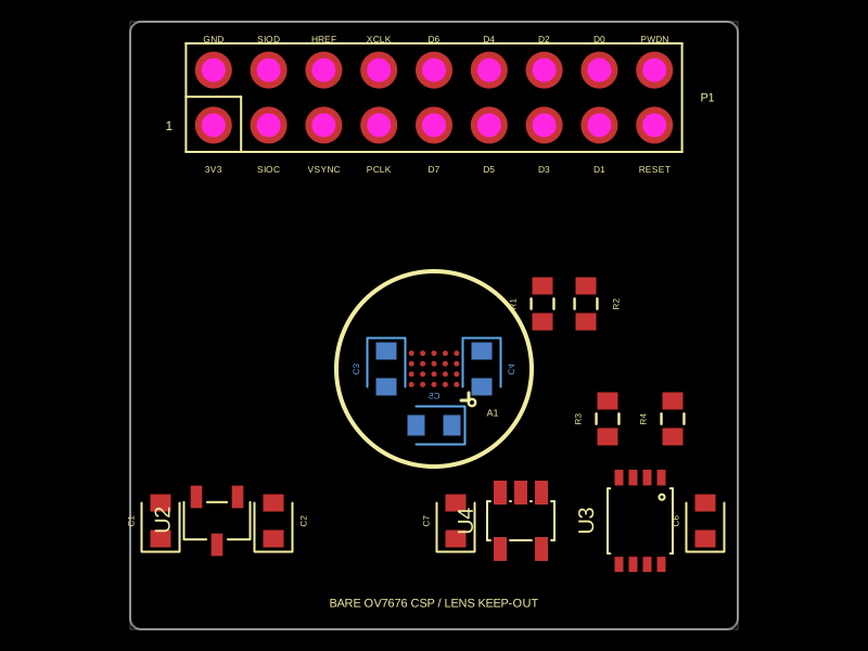
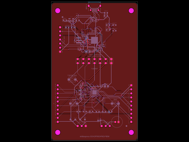
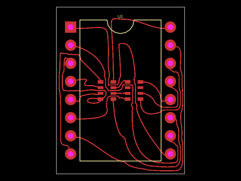
This code defines and integrates a variety of surface-mount, through-hole, and connector hardware components (including microcontrollers, regulators, resistors, capacitors, and connectors) into a PCB design framework, enabling schematic symbol creation, footprint definition, and automated routing within an electronic circuit layout.
- Version
- 1.0.7
- License
- unset
- Stars
- 0
SCHEMATIC_REVIEW.md
# Schematic and design review: ESP32-S3 USB webcam / OV2640

Review date: 2026-08-31

## Verdict

This is a **good engineering-reference schematic, but not a production-ready design**.

- Electrical architecture: **8/10**
- Schematic readability: **8/10 after remediation**
- Verification and testability: **7/10**
- Production readiness: **4/10**
- Overall, for its stated “engineering reference” purpose: **7/10**

The core choices are sensible and unusually well documented: native ESP32-S3 USB, correct USB-C device pull-downs, data-line ESD protection, a protected 5 V input, a properly calculated 3.3 V buck, separate camera rails, boot/reset controls, local decoupling, debug pads, a ground reference plane, and an antenna keepout. Automated connectivity, placement, short-circuit, and routing regression checks pass.

The main reason not to fabricate it as a finished product is that several important claims are not yet closed by the source or by hardware evidence: the exact camera/FPC pinout and mating geometry, camera rail startup behavior, USB impedance, DVP timing/skew, USB current/inrush behavior, and actual UVC streaming. The schematic readability issues found in the initial review have since been remediated.

## What was checked

The cloned project was reviewed from `index.circuit.tsx`, its imported component definitions, the generated Circuit JSON, schematic/PCB renders, README, and the following local commands:

| Check | Result |
| --- | --- |
| `bun run typecheck` | Pass |
| `tsci check netlist` | Pass: 0 errors, 0 warnings in the command output |
| `tsci check schematic-placement` | Pass |
| `tsci check placement` | Pass: 0 placement errors, 0 placement warnings |
| `tsci check shorts index.circuit.tsx` | Pass: no Gerber-derived copper shorts detected |
| `bun test` | Pass: 7 tests, 91 assertions |
| Routing difficulty | Low estimated hotspots; highest reported regions were only a few percent |
| Targeted trace-length inspection | Runs, but important nets contain no encoded trace requirements |

The generated Circuit JSON contains modeling/documentation warnings even though the primary checks pass. Most courtyard warnings concern vias and test pads and are not assembly collisions. The remaining important warnings are underspecified imported pin attributes and imported parts modeled as generic chips; the missing-sheet warning was fixed.

## Strong points

### 1. The system architecture is coherent

The design uses the ESP32-S3's native USB D-/D+ pins on GPIO19/GPIO20. This matches Espressif's documented pin assignment. Avoiding a USB-to-UART bridge reduces parts and lets the same connector serve flashing and UVC operation.

The camera pin mapping is explicitly documented, firmware-ready, and chosen to simplify escape from the module. The design also correctly limits the parallel bus to D2-D9 for 8-bit output and deliberately marks D0, D1, and STROBE unused.

### 2. USB-C device basics are present

CC1 and CC2 each have an independent 5.1 kOhm pull-down, which is the correct basic USB-C sink/device arrangement. D+ and D- have a low-capacitance USBLC6-2SC6 protection array and 33 Ohm series resistors close to the MCU side. The connector shield is coupled to logic ground through 1 MOhm in parallel with a 4.7 nF, 2 kV capacitor rather than being left floating.

### 3. Power topology and component values are plausible

The 3.3 V buck divider gives approximately 3.318 V. Its 2.2 uH / 10 uF output filter and the 6.8 pF feed-forward capacitor agree with the TI TLV62569 guidance for this divider range. The camera rails are nominally appropriate for an OV2640-class module: 2.8 V analog/I/O and about 1.296 V core.

There is local bulk and high-frequency decoupling at the ESP32, regulators, and camera connector. Ground-return vias are deliberately placed near the relevant cells rather than used as incidental stitching.

### 4. The PCB intent is much better documented than average

The source defines four layers, an inner-1 ground plane, an inner-2 3.3 V plane, antenna and mounting-hole keepouts, an ESP32 exposed-pad strategy, top-side-only assembly, camera connector fanout, and fabrication/silkscreen notes. The README honestly identifies the board as provisional and lists concrete bring-up tasks.

### 5. Debug and recovery paths exist

Native USB flashing is supported, while UART0 and JTAG are available on pogo pads. Dedicated BOOT and RESET switches make a bad firmware image recoverable.

## Problems and risks

### High priority before fabrication

#### 1. Camera connector and module compatibility is still assumed

The AFC01-S24FCA-00 footprint, bottom-contact orientation, M0031 pin order, flex insertion depth, and mechanical retention have not been validated with a physical sample. A wrong contact-side or mirrored pinout can damage the camera because three separate supply rails are present on the connector.

**Recommendation:** obtain the exact M0031 and connector, continuity-map all 24 contacts, verify pin 1 and contact side, and do a mechanical insertion test before ordering assembled boards.

#### 2. Camera power-up sequencing and reset recovery are not controlled

The 2.8 V and 1.296 V rails start from the same 3.3 V source through independent LDOs, with no explicit sequencing. Camera RESET_N is permanently pulled high and PWDN permanently low; the ESP32 cannot hold the sensor in reset during rail startup or recover it without cycling the whole board.

This may work, but it is not demonstrated. Camera application guidance commonly requires attention to DOVDD/DVDD/AVDD sequencing when rails are supplied separately.

**Recommendation:** measure all three rails and RESET_N during plug-in, brownout, and reset. Prefer giving the ESP32 control of RESET_N and PWDN, or add a supervisor/sequencing solution if measurement shows unreliable startup.

#### 3. USB impedance and matching are prose requirements, not design constraints

The board says the pair should be 90 Ohm differential, but no final fabrication stackup is selected and the source does not encode a differential-pair impedance or skew requirement. Targeted trace inspection reports `TraceRequirements none`. Connector-side D+ and D- topology is also not geometrically identical because the duplicated Type-C pins are joined differently.

At USB Full-Speed this may still work, but passing connectivity and short checks does not prove signal integrity.

**Recommendation:** select the exact four-layer stackup, calculate the width/gap for 90 Ohm differential, enforce a paired route with a continuous inner-1 return, minimize stubs/vias, and verify D+/D- end-to-end length mismatch.

#### 4. USB current and inrush are not closed

The complete board is powered immediately when VBUS appears: the buck EN is tied high, and the ESP32 plus camera rails can start before USB configuration. The 750 mA PTC protects against gross faults but does not itself establish USB current compliance or controlled inrush.

**Recommendation:** measure plug-in inrush and worst-case steady current, verify the USB descriptors, PTC voltage drop, and regulator headroom, and consider a current-limited load switch/soft-start if required.

### Medium priority

#### 5. DVP timing is not constrained

PCLK, XCLK, VSYNC, HREF, and D2-D9 are routed, but no source-level skew/length constraints are attached. The targeted trace command only exposes individual trace segments because the connector escape and main run are separate traces.

**Recommendation:** extract full end-to-end lengths from Circuit JSON, compare data and sync signals to PCLK, define an acceptable skew budget, and inspect overshoot/ringing on the first prototype. Add source termination footprints if measurements justify them.

#### 6. Schematic readability — resolved

The design now uses two bounded A4 schematic sheets: `SYSTEM + USB` and `CAMERA INTERFACE`. Functional sections were retained and rearranged for consistent signal flow, debug pads were grouped, and notes were added for final-stackup USB impedance verification and the deliberately unused camera pins. Automated placement reports no overlaps, collisions, or out-of-sheet elements; it reports only an optional trace-simplification suggestion for the camera reset pull-up.

#### 7. Reproducibility documentation is currently wrong

The README says the project is pinned and validated with exactly `tscircuit@0.0.2422`, but the cloned `package.json` and `bun.lock` use `^0.0.2461` / `0.0.2461`. A caret range also permits future changes on reinstall.

**Recommendation:** update the README to the actually validated version and use an exact dependency version for release builds. Re-run build, placement, routing, shorts, and visual copper review after any tool upgrade.

#### 8. Imported component models suppress useful electrical checks

Several imported parts are generic `<chip>` components, producing reference-designator and pin-attribute warnings. In particular, some power/ground requirements cannot be checked because the imported models do not declare them.

**Recommendation:** model the connector, fuse, TVS, resistor, and key IC power pins with appropriate semantic elements or complete `pinAttributes`. This will make future netlist checks more meaningful.

### Lower priority / polish

- Add labeled voltage test points for VBUS5V, 3V3, CAM_2V8, and CAM_1V3; current debug pads do not provide convenient access to every rail.
- Recheck BOM availability immediately before ordering; the README stock values are snapshots, not guarantees.
- Validate the external camera envelope, flex bend, lens axis, and enclosure material against the ESP32 antenna keepout.
- Consider adding explicit schematic notes for 3.3 V XCLK into the camera I/O domain and document why it is acceptable for the exact module.
- Resolve or formally waive non-assembly courtyard warnings so the release report distinguishes intentional bare vias/test pads from real component omissions.

## Recommended release gate

Do not call the design production-ready until all of these are complete:

- Physical M0031-to-ZIF continuity and mechanical validation
- Exact stackup and 90 Ohm USB geometry review
- Full end-to-end USB and DVP length/skew report
- Camera rail sequencing and ripple measurements
- USB inrush and worst-case current measurements
- First-article UVC test on Windows, macOS, and Linux
- Thermal test of the buck and both camera LDOs
- RF test with the camera flex and final enclosure installed
- Exact tscircuit version pinned and all generated outputs reviewed again

## Final assessment

The schematic is not bad; electrically it is **well above hobby-demo quality** and shows careful thought. Its strongest feature is that the author already understands most of the remaining risks and records them honestly. Its weakest feature is the gap between a routed, check-clean digital artifact and a physically validated product. Clean netlists and no detected shorts are necessary, but they do not validate connector orientation, analog rail startup, controlled impedance, signal timing, USB compliance, RF behavior, or camera streaming.

For a prototype spin: **reasonable after the connector pinout is independently confirmed**. For a production order: **not yet**.

## Primary references

- [Espressif ESP32-S3-WROOM-1/1U datasheet](https://www.espressif.com/sites/default/files/documentation/esp32-s3-wroom-1_wroom-1u_datasheet_en.pdf)
- [Espressif ESP32-S3 hardware design guidelines](https://documentation.espressif.com/esp-hardware-design-guidelines/en/latest/esp32s3/index.html)
- [TI TLV62569 datasheet](https://www.ti.com/lit/ds/symlink/tlv62569.pdf)
- [ST USBLC6-2SC6 documentation](https://www.st.com/content/st_com/en/technical-documents/DS4260.html)
- [OV2640 FSL module datasheet mirror](https://www.mpja.net/download/ov2640data%20sheet.pdf)