README.md
# STM32 MIDI keys — PCB-only tscircuit recreation

The project contains the original 170 × 60 mm, two-layer, 1.6 mm PCB as a
converted Circuit JSON reference and a native TSX version using tscircuit's
autorouter. Schematic generation is disabled in both the board and project config.

**Status: PCB recreation and routing investigation, not a verified fabrication
release.** High-priority importer, keepout/pour, and routing failures are recorded
in [ISSUES.md](ISSUES.md), with local evidence. The original board also has KiCad
DRC findings. Do not interpret a rendered preview as a clean DRC result.

The current native run completes **two routing phases**, producing **169 PCB
traces and 240 vias**. All 86 components, all 14 touch-electrode nets, and all
241 connected physical pad assignments are preserved. There are no reported
unconnected-port errors. Six DRC errors remain: three via-hole/SMD-pad overlaps,
two crystal-net via-count violations, and a ground-net length-limit violation.
The build therefore exits nonzero. See `validation/summary.json` and
`validation/native-autoroute.log`.
The original track/via-only key-area keepout also remains unsupported: one KEY_AS
route extends below the electronics strip. See the keepout findings in `ISSUES.md`.

The board now instantiates **35 JLCPCB-imported components across 66 placements**.
See [COMPONENTS.md](COMPONENTS.md) and `source/jlcpcb-bom.json`. BZ1 remains
unsourced because the original only says Speaker/Piezo and a matching part has
not been verified. PCB electrodes, holes, and the solder jumper are not purchased
components.

## Open and build

```sh
bun install
bun run dev                 # native TSX PCB with phased autorouting
bun run dev:reference       # converted source routing for comparison
bun run check               # netlist, then component placement
bun run build               # actual autorouting, phase artifacts, PCB images
bun run preview             # top/bottom images for both versions
```

The build command intentionally exits nonzero when final DRC finds errors.
It does not suppress electrical errors or replace autorouted output with the
original tracks. Build files and diagnostics are still saved for investigation.

## Native design

[`index.circuit.tsx`](index.circuit.tsx) fixes all 86 component positions and
uses source-derived footprints, explicit nets/traces, native copper pours, and
two `<autoroutingphase>` elements with `auto_local`:

1. USB and crystal/clock connections.
2. Touch sensing, control, expansion, audio, ground, and supply rails together.

Combining the remaining nets in one phase avoids the fixed-route fallback crash
seen with four phases. Earlier failures remain documented in `ISSUES.md`.

Each phase consumes previous-phase routes. No source KiCad tracks/vias are fed
to this autorouter. Each saved phase input/output is in `dist/autorouter-debug/`.
USB routing here does not claim verified differential impedance or length matching.
`autorouted.circuit.json` is the saved native output, including its DRC errors;
it is separate from the original KiCad routing reference.

Pre-routing netlist and placement DRC report zero errors/warnings. The placement
command still exits nonzero because its separate routing-difficulty heuristics
suggest rotating source components; the requested original pad positions and
net assignments are deliberately preserved. No DRC checks are disabled.

## Preserved reference and verification

- `source/stm32_midi_keys.kicad_pcb`: byte-for-byte copy of the supplied board.
- `board.circuit.json`: corrected conversion, retaining original copper routing.
- `reference.circuit.json`: that conversion plus restored filled key silkscreen.
- `source/geometry.json`: independently parsed source geometry and net memberships.
- `source/pad-shapes.json`: copper offsets/custom-pad unions from KiCad's own API.
- `validation/import-parity.json`: all 86 component positions and ordinary pad
  centers matched; all 1,104 source segments, 124 vias, and 29 saved copper-fill
  polygons retained. Offset pad centers are checked against KiCad's shape centers.
- `validation/kicad-drc.json`: DRC against the untouched original source.
- `validation/autoroute.log`: actual phase progress and final native build findings.
- `validation/summary.json`: native pad/hole positions match the corrected
  reference; zero schematic elements; all 14 electrode nets present; routing errors.
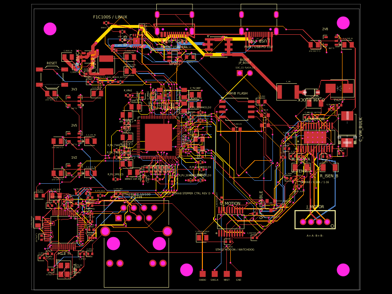
- `previews/`: top/bottom PCB images; reference and native placement are labeled separately.

Regenerate conversion and check its geometry:

```sh
bun run import:board
bun run verify:import
bun run preview
bun run build:reference
```

The recorded special-pad geometry is included so rebuilding does not require
KiCad. To regenerate it, run `scripts/kicad_pad_shapes.py` with a Python runtime
that has `pcbnew` installed; on this Mac it is KiCad's bundled Python 3.9.

## Fidelity limits and explicit differences

The source copper routes are retained in the reference; the native version
autoroutes fresh paths. The native ground outlines are clipped away from the
rounded board corners to address the original ground-region clearance issue.
Its electrode `unbroken` pours/routing regions are a workaround, not an exact
translation of KiCad's both-layer, track/via-only keepouts.

Circuit JSON does not provide filled silkscreen polygons in this version. The
14 source polygons are approximated with merged 0.025 mm horizontal strips.
Rounded board arcs are polygonized by the importer. Fonts, some pad rounding,
solder-mask/paste metadata, fabrication graphics, and custom 3D models are not
certified identical. This project does **not** claim a manufacturing-exact
round trip; retain the original KiCad file as the authoritative source.

This is a development package. No fabrication orders have been placed; the native routing is not fabrication-ready.