mohan-bee/stm32-midi-keys
Clips rectangular ground-region geometry to fit within the board’s scaled rounded-edge outline using polygon intersection.
- Version
- 1.0.2
- License
- unset
- Stars
- 0
index.circuit.tsx
PCB
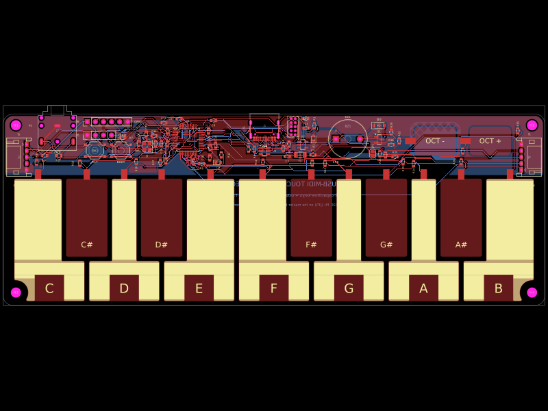
Schematic

import imported from './board.circuit.json'
import geometry from './source/geometry.json'
import { transformPCBElements } from '@tscircuit/circuit-json-util'
import { translate } from 'transformation-matrix'
import silk from './silkscreen.json'
import { clipGroundOutline } from './clip-ground-outline'
import { jlcpcbComponents } from './jlcpcb-components'
import { TopAccessFootprint } from './top-access-footprint'

const board = imported.find(e => e.type === 'pcb_board')!
// Keep source footprints and positions, but let tscircuit route every net.
const components = new Map(imported.filter(e => e.type === 'source_component').map(e => [e.source_component_id, e]))
const nets = imported.filter(e => e.type === 'source_net')
const netName = (name: string) => name.replace(/\+/g,'_P').replace(/-/g,'_').replace(/[^A-Za-z0-9_]/g,'_').replace(/_+/g,'_').replace(/^_+|_+$/g,'')
const netPins = new Map<string,string[]>()
const footprints = imported.filter(e => e.type === 'pcb_component').map(c => {
  const source = components.get(c.source_component_id)!
  const original = geometry.footprints.find(f=>f.name===source.name)!
  const elements = structuredClone(imported.filter(e => e.pcb_component_id === c.pcb_component_id && !['pcb_component','pcb_port','pcb_silkscreen_text'].includes(e.type)))
  transformPCBElements(elements, translate(-c.center.x, -c.center.y))
  for(const e of elements) if(e.type==='pcb_smtpad' && e.shape==='rect') e.rect_border_radius=e.corner_radius
  const pads = elements.filter(e=>['pcb_smtpad','pcb_plated_hole'].includes(e.type))
  const pinLabels: Record<string,string[]> = {}
  pads.forEach((pad,i)=>{
    const originalNumber=pad.port_hints![0]
    const pin=`pin${i+1}`
    const name=original.pads.find(p=>p.number===originalNumber)?.net
    pinLabels[pin]=[`kicad_${originalNumber}_pad${i+1}`]
    pad.port_hints=[pin]
    delete pad.pcb_port_id
    if(name) {const n=netName(name);netPins.set(n,[...(netPins.get(n)??[]),`${source.name}.${pin}`])}
  })
  return {source, c, elements, pinLabels}
})
const phase = (name: string) => /USB|OSC/.test(name) ? 0 : 1
const traces = [...netPins].map(([name,pins])=>({name,pins}))
// Unbroken pours reserve the top-side electrodes. The original track/via-only
// keepout is not equivalent to a native keepout (see ISSUES.md).

export default function Stm32MidiKeys() {
  return <board outline={board.outline} width={170} height={60}
    thickness={1.6} layers={2} schematicDisabled autorouterVersion="latest"
    defaultTraceWidth={0.2} minTraceWidth={0.15} minBoardEdgeClearance={0.2}>
    {footprints.map(({source,c,elements,pinLabels}) => {
      const Component = jlcpcbComponents[source.name as keyof typeof jlcpcbComponents] ?? 'chip'
      const touchPad = source.name.startsWith('TK') ? elements.find(e=>e.type==='pcb_smtpad') : null
      const footprint = touchPad ? <footprint><smtpad shape="rect" pcbX={touchPad.x} pcbY={touchPad.y}
        width={touchPad.width} height={touchPad.height} portHints={touchPad.port_hints} coveredWithSolderMask /></footprint>
        : ['J2','J5','J6','JP1'].includes(source.name)
          ? <TopAccessFootprint elements={elements} /> : elements
      return <Component key={source.name} name={source.name} resistance={source.resistance} capacitance={source.capacitance}
        {...(source.name === 'Y1' ? {maxTraceLength: 50} : {})}
        {...(source.ftype === 'simple_capacitor' ? {maxDecouplingTraceLength: 300} : {})}
        pcbX={c.center.x} pcbY={c.center.y} footprint={footprint} pinLabels={pinLabels} symbol={undefined}
        pcbStyle={{silkscreenTextVisibility:'hidden'}} />
    })}
    {imported.filter(e=>e.type==='pcb_silkscreen_text').map(e=><silkscreentext key={e.pcb_silkscreen_text_id}
      text={e.text} pcbX={e.anchor_position.x} pcbY={e.anchor_position.y} pcbRotation={e.ccw_rotation ?? 0}
      anchorAlignment={e.anchor_alignment} fontSize={e.font_size} layer={e.layer} />)}
    {silk.map(e=><silkscreenrect key={e.pcb_silkscreen_rect_id} pcbX={e.center.x} pcbY={e.center.y}
      width={e.width} height={e.height} layer={e.layer} filled strokeWidth={0} />)}
    <autoroutingphase name="usb-and-clock" phaseIndex={0} autorouter="auto_local" />
    <autoroutingphase name="touch-control-and-power" phaseIndex={1} autorouter="auto_local" />
    {nets.map(n => <net key={n.name} name={n.name} routingPhaseIndex={phase(n.name)} />)}
    {traces.filter(t => !t.name.startsWith('unconnected')).map(t => <trace key={t.name} path={[...t.pins, `net.${t.name}`]} routingPhaseIndex={phase(t.name)} />)}
    {geometry.zones.filter(z => z.net).map((z,i) => <copperpour key={i}
      name={z.name || `${z.layer}-ground`} layer={z.layer === 'F.Cu' ? 'top' : 'bottom'}
      connectsTo={`net.${netName(z.net)}`} outline={z.net==='GND' && !z.name ? clipGroundOutline(z.outline,board.outline) : z.outline}
      unbroken={z.name.startsWith('TOUCH_')}
      crosshatch={z.name === 'GND_hatch_under_touch_keys'} crosshatchPitch={1.8} crosshatchWidth={0.3}
      clearance={z.name.startsWith('TOUCH_') ? 0 : 0.4} boardEdgeMargin={0.25} coveredWithSolderMask />)}
  </board>
}
Related Packages
 More from this authormohan-bee/rp2040-crystalThis design features a 12MHz crystal oscillator with two 18pF load capacitors connected to its XIN and XOUT pins, mounted on a PCB with associated grounding traces.
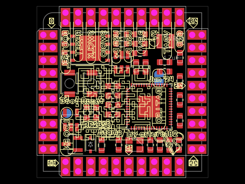 Similar packagetechmannih/imported-rp2350-stamp-boardThis code defines a detailed PCB layout with multiple layers, including the physical outline, component footprints, drilling holes, SMT pads, silkscreen markings, and courtyard outlines for component placement and board edges.
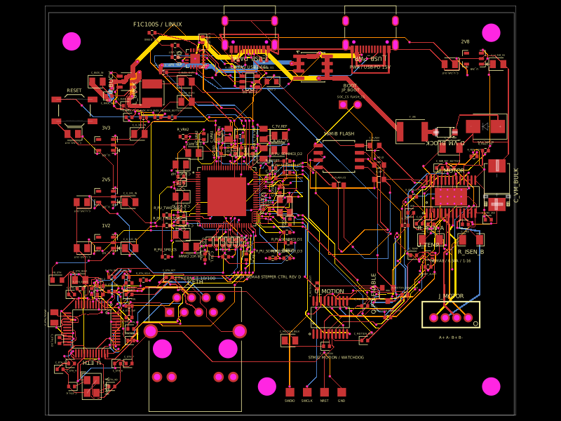 Discover something newshibosoftwaredev/f1c100s-linux-nema8-stepper-controllerRestores component part numbers and CAD models, removes test-point 3D bodies, and validates that solder paste exists only on top-side SMT pads without altering copper or DRC.