mohan-bee/stm32-midi-keys
Clips rectangular ground-region geometry to fit within the board’s scaled rounded-edge outline using polygon intersection.
- Version
- 1.0.2
- License
- unset
- Stars
- 0
top-access-footprint.tsx
PCB

Schematic

// Native primitives let the vertical headers/jumper declare their access direction.
export function TopAccessFootprint({elements}: {elements: any[]}) {
  // The KiCad converter emits each courtyard edge as a two-point outline.
  // Native courtyardoutline expects a closed polygon, so reconnect those edges.
  const edges = elements.filter(e=>e.type==='pcb_courtyard_outline').map(e=>e.outline)
  const courtyard = edges.shift()?.slice() ?? []
  while(edges.length && courtyard.length) {
    const end = courtyard[courtyard.length-1]
    const same = (p: any) => Math.hypot(p.x-end.x,p.y-end.y)<1e-6
    const index = edges.findIndex(edge=>same(edge[0]) || same(edge[edge.length-1]))
    if(index<0) break
    const edge=edges.splice(index,1)[0]
    courtyard.push(...(same(edge[0]) ? edge : edge.slice().reverse()).slice(1))
  }
  return <footprint insertionDirection="from_above">
    {courtyard.length>=3 && <courtyardoutline outline={courtyard} layer="top" />}
    {elements.map((e, i) => {
      if (e.type === 'pcb_smtpad' && e.shape === 'polygon')
        return <smtpad key={i} shape="polygon" points={e.points} portHints={e.port_hints} layer={e.layer} />
      if (e.type === 'pcb_plated_hole') {
        if(e.shape === 'circular_hole_with_rect_pad')
          return <platedhole key={i} shape={e.shape} pcbX={e.x} pcbY={e.y}
            holeDiameter={e.hole_diameter} rectPadWidth={e.rect_pad_width} rectPadHeight={e.rect_pad_height}
            holeOffsetX={e.hole_offset_x ?? 0} holeOffsetY={e.hole_offset_y ?? 0}
            pcbRotation={e.rect_ccw_rotation} portHints={e.port_hints} />
        return <platedhole key={i} shape="pill" pcbX={e.x} pcbY={e.y}
          holeWidth={e.hole_width} holeHeight={e.hole_height} outerWidth={e.outer_width} outerHeight={e.outer_height}
          pcbRotation={e.ccw_rotation} portHints={e.port_hints} />
      }
      if(e.type === 'pcb_silkscreen_path')
        return <silkscreenpath key={i} route={e.route} strokeWidth={e.stroke_width} layer={e.layer} />
      if(e.type === 'pcb_fabrication_note_path')
        return <fabricationnotepath key={i} route={e.route} strokeWidth={e.stroke_width} layer={e.layer} />
      return null
    })}
  </footprint>
}
Related Packages
 More from this authormohan-bee/rp2040-crystalThis design features a 12MHz crystal oscillator with two 18pF load capacitors connected to its XIN and XOUT pins, mounted on a PCB with associated grounding traces.
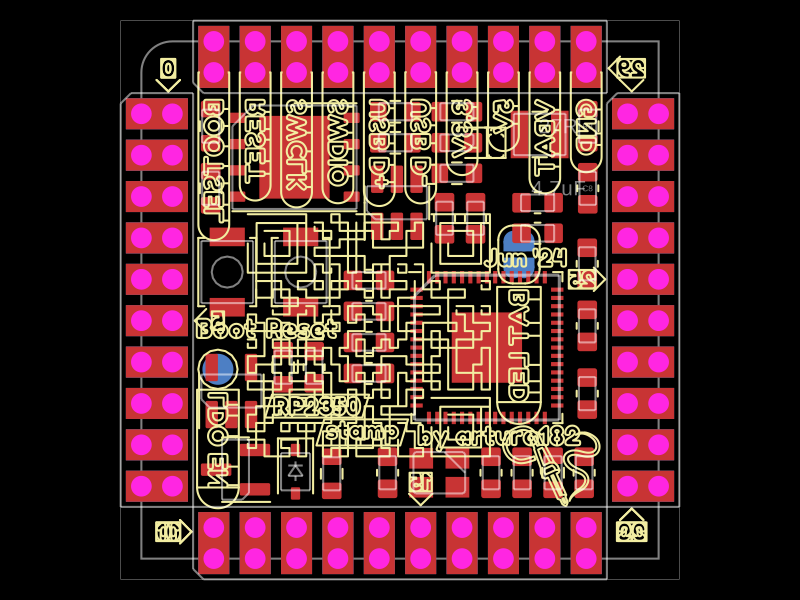 Similar packagetechmannih/imported-rp2350-stamp-boardThis code defines a detailed PCB layout with multiple layers, including the physical outline, component footprints, drilling holes, SMT pads, silkscreen markings, and courtyard outlines for component placement and board edges.
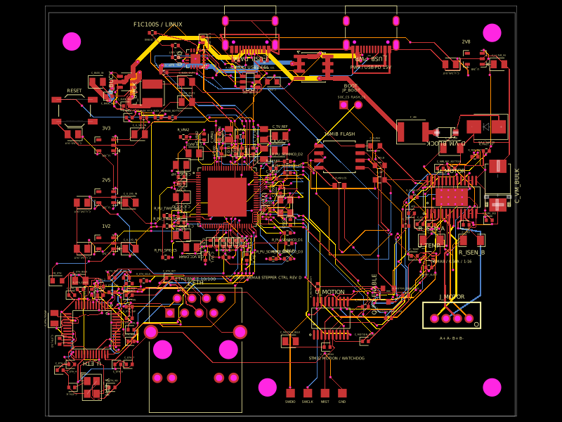 Discover something newshibosoftwaredev/f1c100s-linux-nema8-stepper-controllerRestores component part numbers and CAD models, removes test-point 3D bodies, and validates that solder paste exists only on top-side SMT pads without altering copper or DRC.