README.md
# Four gang WiFi switch — ordinary pin headers, THT DNP

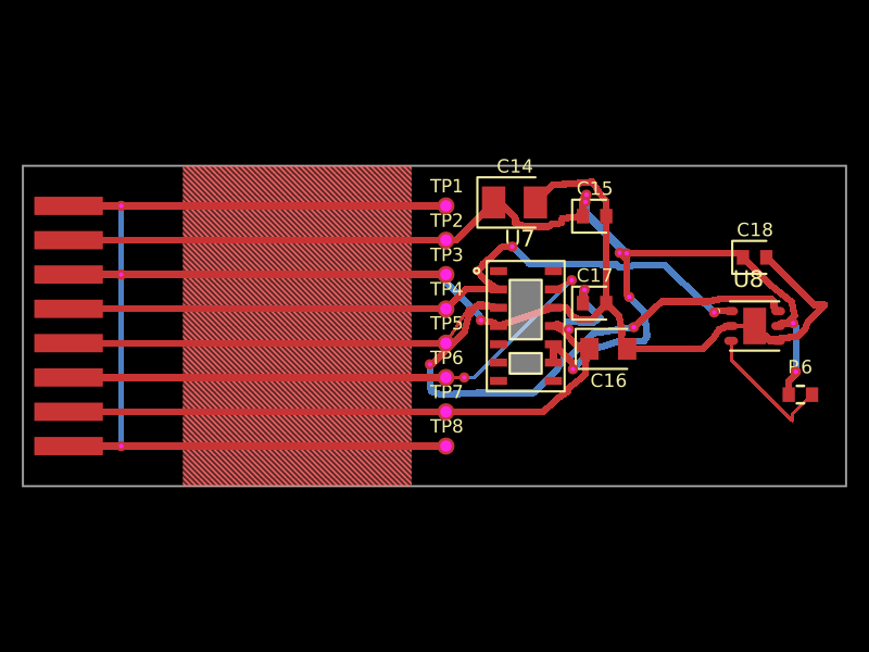
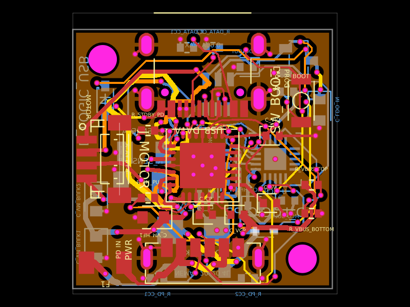
Two 48 × 50 mm, two-layer prototype PCBs. Every component remains on the top side. The controller retains ESP-12F and the ready-made isolated HLK-5M05 supply; the relay board retains four HF32F-G relays.

All external connectors are **ordinary straight, unshrouded male pin headers**:

| Connection | Part | JLCPCB ID | Pitch |
|---|---|---|---:|
| AC L/N headers, 2 pins | XFCN PZ508V-11-02P-H25 | C25170858 | 5.08 mm |
| Switched outputs, 4 pins | XFCN PZ508V-11-04P-H25 | C41355716 | 5.08 mm |
| Control/programming, 6 pins | HJ Tech 17-0020-002 | C6800644 | 2.54 mm |

The AC/output headers use 5.08 mm pitch to retain the design's mains copper spacing target. Their stock footprints have approximately 2.78/2.88 mm adjacent pad gaps. The [XFCN drawing](https://www.xfconn.com/uploads/soft/20240902/4-240Z214563b63.pdf) specifies 1.6 mm PCB holes and body sizes of 10.16 × 6.35 mm / 20.32 × 6.35 mm. Explicit courtyards include those plastic bodies, which the imported footprint's copper-only dimensions do not describe.

**AC pinout changed:** each AC header now has only two pins: **1 = L, 2 = N**. The previous three-pin connector's unused middle position has been removed. Use the matching new header arrangement when making cables.

## DNP and assembly

Every through-hole component has tscircuit's supported `doNotPlace` flag. It becomes `pcb_component.do_not_place=true`. This excludes the part from factory pick-and-place while retaining its footprint, holes, net connections and routing.

| Board | Factory DNP / manual fit later | SMT factory population |
|---|---|---|
| Controller | PS1, F1, RV1, J_AC, J_LINK, J_PROG | U1, U2, C1–C5, R1–R5 |
| Relay | K1–K4, J_AC_IN, J_AC_PWR, J_OUT, J_LINK | U1, C1, C2 |

**DNP parts are required for the completed switch.** Fit them manually after SMT assembly. The factory-populated boards alone are incomplete. DNP components may be absent in the 3D preview because core omits their CAD models; their PCB pads and holes remain.

`bom.csv` is the master list including population status. `assembly/*-smt-bom.csv` and `assembly/*-smt-cpl.csv` contain only SMT factory parts. `assembly/*-tht-manual-fit.csv` lists the omitted through-hole parts for later fitting. These are draft assembly outputs; no fabrication order has been placed.

The assembly audit checks exact THT DNP / SMT population, all-top placement, normal header types, retained physical pads/ports and exact pick-and-place population. It also runs placement checks on a clone with DNP flags cleared, so factory omissions do not hide overlaps in the eventual hand-fitted assembly.

## Routing and checks

Fresh routing uses the official default **`@tscircuit/capacity-autorouter` 0.0.1027**, `AutoroutingPipelineSolver` / Pipeline9, through `default-capacity.ts`. Each attempt routes all connections in its phase together. The adapter supplies constraints and validates candidates without authoring or moving copper centerlines. No saved board copper paths are imported. Explicit `autoroutingphase`s are used; `routeRemaining={false}` prevents an additional fallback phase.

Relay mains phases set `preserveHighDensityPaths:true`: the adapter disables the current trace-simplification pass because it can lose the configured wide-trace pad clearance. The paths come from the default capacity high-density solver; later solver stages and all final physical checks remain active. This is a targeted configuration workaround, rather than a claim that every stage runs with stock settings.

The project uses `schAutoLayoutEnabled` without manual schematic X/Y coordinates. Isolation strips and the ESP antenna keepout remain.

The relay live bus prefers 2.4 mm and permits 2.2 mm minimum; outputs are 1.5 mm and supply neutral 0.8 mm. Relay low-voltage power permits 0.35 mm, signals 0.25 mm. Controller supply routes are 0.8 mm; controller rails prefer 0.4 mm but permit real 0.2 mm sections. These are geometry rules, not verified current ratings.

`proof/` includes raw Circuit JSON, phase inputs/outputs, source hashes, routing validation and assembly audits. Native routing, independent copper spacing, keepouts, endpoint connectivity, physical via drills and actual outgoing trace widths are checked. Core may reverse some via direction labels; raw data is retained and the audit verifies physical coordinates, nets and layer spans before normalizing labels only for its independent check.

## Build and inspect

```sh
bun install
bun run test:router
bun run build
bun run capture:controller
bun run capture:relay
bun run validate:controller
bun run validate:relay
bun run audit:controller
bun run audit:relay
python3 -m http.server 8771 --directory dist
```

Build runs `tsci build --site --pcb-svgs --pcb-png`. Both boards are available at `http://127.0.0.1:8771`.

## Header connections

| Header | Pin order |
|---|---|
| Both J_LINK | 1: +5 V, 2: GND, 3–6: CH1–CH4 |
| Relay J_AC_IN | 1: live input, 2: neutral input |
| Relay J_AC_PWR | 1: live to controller, 2: neutral to controller |
| Controller J_AC | 1: live from relay, 2: neutral from relay |
| Relay J_OUT | 1–4: switched live channels 1–4 |
| Controller J_PROG | 1: GND, 2: 3.3 V, 3: ESP TX, 4: ESP RX, 5: BOOT, 6: RESET |

Use separate cables for mains and control. Load neutral distribution is external. Direct stacking and spacer height remain unspecified. ESP GPIO4/5/12/13 control channels 1/2/3/4, active high. Programming uses 3.3 V logic. Firmware and wall-switch inputs are outside this design.

## Prototype limits

**This revision is not released for household mains use or manufacturing.** Contact catalog ratings do not qualify the board. Insulation, accessible live pins, enclosure, protection, load/inrush behavior, RF/EMC, assembly tolerances and temperature need engineering review and testing. The earlier draft 2 A/channel and 4 A total target is unverified. The controller fuse protects only its supply branch.

The AP2112 regulator and ESP supply transients are untested; 500 mA from 5 V to 3.3 V would dissipate 0.85 W in the regulator. Some controller power/GND copper is 0.2 mm wide. Catalog IDs do not guarantee JLCPCB stock. Matching cables, upstream protection and a verified Gerber/drill fabrication package are not included.