mohan-bee/four-gang-wifi-switch-layout
A tscircuit package created by mohan-bee.
- Version
- 0.0.9
- License
- unset
- Stars
- 0
controller.circuit.tsx
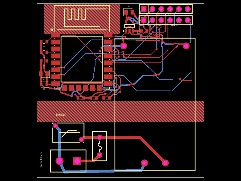
PCB
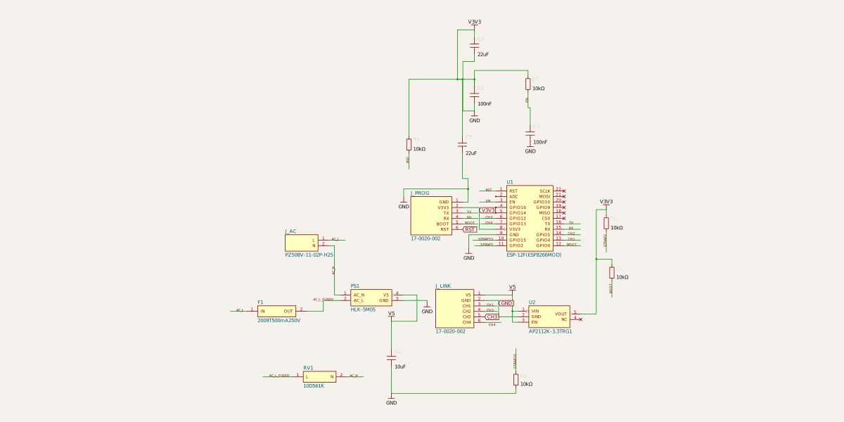
Schematic
import { defaultCapacity } from "./default-capacity"
// 48 x 50 mm controller/power PCB. Draft routing; isolated 5V supply branch only.
// JLC footprints retain EasyEDA pad numbering, including the ESP-12F's 9=GND.
export default function ControllerBoard() {
  return (
    <board width={48} height={50} layers={2} thickness={1.6} doubleSidedAssembly={false}
      title="4 gang WiFi - controller and power" autorouter="auto_local" routeRemaining={false} autorouterVersion="beta_pipeline9" minViaPadDiameter={0.6} minViaHoleDiameter={0.3} minTraceWidth={0.2} minTraceToPadEdgeClearance={0.2} minViaEdgeToPadEdgeClearance={0.2} minPadEdgeToPadEdgeClearance={0.2} minViaHoleEdgeToViaHoleEdgeClearance={0.2} minBoardEdgeClearance={0.5} schAutoLayoutEnabled>

      <net name="AC_L" nominalTraceWidth={0.8} routingPhaseIndex={1} />
      <net name="AC_L_FUSED" nominalTraceWidth={0.8} routingPhaseIndex={1} />
      <net name="AC_N" nominalTraceWidth={0.8} routingPhaseIndex={0} />
      <net name="V5" nominalTraceWidth={0.4} routingPhaseIndex={2} />
      <net name="GND" nominalTraceWidth={0.4} routingPhaseIndex={2} />
      <net name="V3V3" nominalTraceWidth={0.4} routingPhaseIndex={2} />
      {["EN","RST","BOOT","STRAP2","STRAP15","CH1","CH2","CH3","CH4","TX","RX"].map(name =>
        <net key={name} name={name} nominalTraceWidth={0.2} routingPhaseIndex={2} />)}
      <autoroutingphase name="SUPPLY_NEUTRAL" phaseIndex={0} algorithmFn={defaultCapacity({name:"controller-SUPPLY_NEUTRAL",side:"below",layer:"bottom",guardPhysicalEdges:true})} minTraceWidth={0.8} minTraceToPadEdgeClearance={1.5} minViaEdgeToPadEdgeClearance={1.5} minBoardEdgeClearance={0.75} />
      <autoroutingphase name="MAINS_LIVE" phaseIndex={1}
        algorithmFn={defaultCapacity({name:"controller-MAINS_LIVE",side:"below",layer:"top"})}
        minTraceWidth={0.8} minTraceToPadEdgeClearance={1.5}
        minViaEdgeToPadEdgeClearance={1.5} minBoardEdgeClearance={0.75} />
      <autoroutingphase name="JOINT_LV" phaseIndex={2} minTraceWidth={0.2} algorithmFn={defaultCapacity({name:"controller-joint-lv",side:"above",viaPlanningMargin:0.12})} />
      <chip layer="top" name="U1" manufacturerPartNumber="ESP-12F(ESP8266MOD)"
        footprint="jlcpcb:C82891" supplierPartNumbers={{ jlcpcb: ["C82891"] }}
        pcbX={-11.1} pcbY={8.2} pcbRotation={-90}
        pinLabels={{ pin1:"RST", pin2:"ADC", pin3:"EN", pin4:"GPIO16", pin5:"GPIO14", pin6:"GPIO12", pin7:"GPIO13", pin8:"V3V3", pin9:"GND", pin10:"GPIO15", pin11:"GPIO2", pin12:"GPIO0", pin13:"GPIO4", pin14:"GPIO5", pin15:"RX", pin16:"TX", pin17:"CS0", pin18:"MISO", pin19:"GPIO9", pin20:"GPIO10", pin21:"MOSI", pin22:"SCLK" }}
        pinAttributes={{ V3V3:{requiresPower:true,requiresVoltage:3.3}, GND:{requiresGround:true}, CS0:{doNotConnect:true}, MISO:{doNotConnect:true}, GPIO9:{doNotConnect:true}, GPIO10:{doNotConnect:true}, MOSI:{doNotConnect:true}, SCLK:{doNotConnect:true} }}
        connections={{ V3V3:"net.V3V3", GND:"net.GND", EN:"net.EN", RST:"net.RST", GPIO0:"net.BOOT", GPIO2:"net.STRAP2", GPIO15:"net.STRAP15", GPIO4:"net.CH1", GPIO5:"net.CH2", GPIO12:"net.CH3", GPIO13:"net.CH4", TX:"net.TX", RX:"net.RX" }} />

      <chip layer="top" doNotPlace name="PS1" manufacturerPartNumber="HLK-5M05"
        footprint="jlcpcb:C209907" supplierPartNumbers={{ jlcpcb:["C209907"] }}
        pcbX={9.9} pcbY={-4} pcbRotation={90}
        pinLabels={{ pin1:"AC_N", pin2:"AC_L", pin3:"GND", pin4:"V5" }}
        pinAttributes={{ V5:{providesPower:true,providesVoltage:5}, GND:{providesGround:true} }}
        connections={{ AC_N:"net.AC_N", AC_L:"net.AC_L_FUSED", GND:"net.GND", V5:"net.V5" }} />

      <chip layer="top" name="U2" manufacturerPartNumber="AP2112K-3.3TRG1"
        footprint="jlcpcb:C51118" supplierPartNumbers={{ jlcpcb:["C51118"] }}
        pcbX={2.6} pcbY={18.5}
        pinLabels={{pin1:"VIN",pin2:"GND",pin3:"EN",pin4:"NC",pin5:"VOUT"}}
        pinAttributes={{VIN:{requiresPower:true,requiresVoltage:5},GND:{requiresGround:true},VOUT:{providesPower:true,providesVoltage:3.3},NC:{doNotConnect:true}}}
        connections={{VIN:"net.V5",GND:"net.GND",EN:"net.V5",VOUT:"net.V3V3"}} />
      <capacitor name="C1" capacitance="10uF" voltageRating={10} footprint="0603" supplierPartNumbers={{jlcpcb:["C19702"]}} pcbX={6.8} pcbY={17.1} layer="top" connections={{pin1:"net.V5",pin2:"net.GND"}} />
      <capacitor name="C2" capacitance="22uF" voltageRating={25} footprint="0805" supplierPartNumbers={{jlcpcb:["C45783"]}} pcbX={2.5} pcbY={22.5} layer="top" connections={{pin1:"net.V3V3",pin2:"net.GND"}} />
      <capacitor name="C3" capacitance="100nF" voltageRating={50} footprint="0603" supplierPartNumbers={{jlcpcb:["C14663"]}} pcbX={-22} pcbY={1.8} pcbRotation={180} layer="top" connections={{pin1:"net.V3V3",pin2:"net.GND"}} />
      <capacitor name="C4" capacitance="22uF" voltageRating={25} footprint="0805" supplierPartNumbers={{jlcpcb:["C45783"]}} pcbX={-22} pcbY={4.8} pcbRotation={180} layer="top" connections={{pin1:"net.V3V3",pin2:"net.GND"}} />
      <capacitor name="C5" capacitance="100nF" voltageRating={50} footprint="0603" supplierPartNumbers={{jlcpcb:["C14663"]}} pcbX={-22} pcbY={8.5} layer="top" pcbRotation={180} connections={{pin1:"net.EN",pin2:"net.GND"}} />

      {[
        {name:"R1",x:-22,y:11,net:"EN",pull:"V3V3",rotation:180},
        {name:"R2",x:-22,y:14,net:"RST",pull:"V3V3",rotation:180},
        {name:"R3",x:-11.4,y:-2.15,net:"BOOT",pull:"V3V3",rotation:0},
        {name:"R4",x:-7.7,y:-2.15,net:"STRAP2",pull:"V3V3",rotation:180},
        {name:"R5",x:-4,y:-2.15,net:"STRAP15",pull:"GND",rotation:0},
      ].map(r => <resistor key={r.name} name={r.name} resistance="10k" footprint="0603" supplierPartNumbers={{jlcpcb:["C25804"]}} pcbX={r.x} pcbY={r.y} layer="top" pcbRotation={r.rotation} connections={{pin1:`net.${r.net}`,pin2:`net.${r.pull}`}} />)}

      <pinheader pinCount={2} gender="male" layer="top" doNotPlace name="J_AC" manufacturerPartNumber="PZ508V-11-02P-H25" footprint="jlcpcb:C25170858" supplierPartNumbers={{jlcpcb:["C25170858"]}}
        pcbX={-15} pcbY={-20.25} pcbRotation={180} pinLabels={{pin1:"L",pin2:"N"}}
        connections={{L:"net.AC_L",N:"net.AC_N"}}>
        {/* Manufacturer body 10.16 x 6.35mm; include a 0.25mm courtyard margin. */}
        <courtyardrect pcbX={0} pcbY={0} width={10.66} height={6.85} />
      </pinheader>
      <chip layer="top" doNotPlace name="F1" manufacturerPartNumber="2009T500mA250V" footprint="jlcpcb:C529783" supplierPartNumbers={{jlcpcb:["C529783"]}}
        pcbX={-6} pcbY={-16} pcbRotation={90} pinLabels={{pin1:"IN",pin2:"OUT"}}
        connections={{IN:"net.AC_L",OUT:"net.AC_L_FUSED"}} />
      <chip layer="top" doNotPlace name="RV1" manufacturerPartNumber="10D561K" footprint="jlcpcb:C2839517" supplierPartNumbers={{jlcpcb:["C2839517"]}}
        pcbX={-15} pcbY={-12.1} pcbRotation={180} pinLabels={{pin1:"L",pin2:"N"}}
        connections={{L:"net.AC_L_FUSED",N:"net.AC_N"}} />
      <pinheader pinCount={6} gender="male" layer="top" doNotPlace name="J_LINK" manufacturerPartNumber="17-0020-002" footprint="jlcpcb:C6800644" supplierPartNumbers={{jlcpcb:["C6800644"]}}
        pcbX={13} pcbY={23.4} pinLabels={{pin1:"V5",pin2:"GND",pin3:"CH1",pin4:"CH2",pin5:"CH3",pin6:"CH4"}}
        connections={{V5:"net.V5",GND:"net.GND",CH1:"net.CH1",CH2:"net.CH2",CH3:"net.CH3",CH4:"net.CH4"}} />
      <pinheader pinCount={6} gender="male" layer="top" doNotPlace name="J_PROG" manufacturerPartNumber="17-0020-002" footprint="jlcpcb:C6800644" supplierPartNumbers={{jlcpcb:["C6800644"]}}
        pcbX={13} pcbY={20.2} pinLabels={{pin1:"GND",pin2:"V3V3",pin3:"TX",pin4:"RX",pin5:"BOOT",pin6:"RST"}}
        connections={{GND:"net.GND",V3V3:"net.V3V3",TX:"net.TX",RX:"net.RX",BOOT:"net.BOOT",RST:"net.RST"}} />

      {/* Copper-free isolation strip; only the encapsulated isolated supply bridges it. */}
      <keepout shape="rect" pcbX={0} pcbY={-6} width={48} height={6} layers={["top","bottom"]} excludeRefs={[".PS1"]} />
      <keepout shape="rect" pcbX={-11.1} pcbY={20.5} width={22} height={8.5} layers={["top","bottom"]} excludeRefs={[".U1"]} />
      <silkscreentext text="5V G 1 2 3 4" pcbX={13} pcbY={21.8} fontSize={0.8} />
      <silkscreentext text="PROG G 3 TX RX B R" pcbX={13} pcbY={18.8} fontSize={0.65} />
      <silkscreentext text="AC IN 1:L 2:N" pcbX={-22.9} pcbY={-19.8} pcbRotation={90} fontSize={0.65} />
      <silkscreentext text="MAINS" pcbX={-17} pcbY={-7} fontSize={0.9} />
    </board>
  )
}
Related Packages
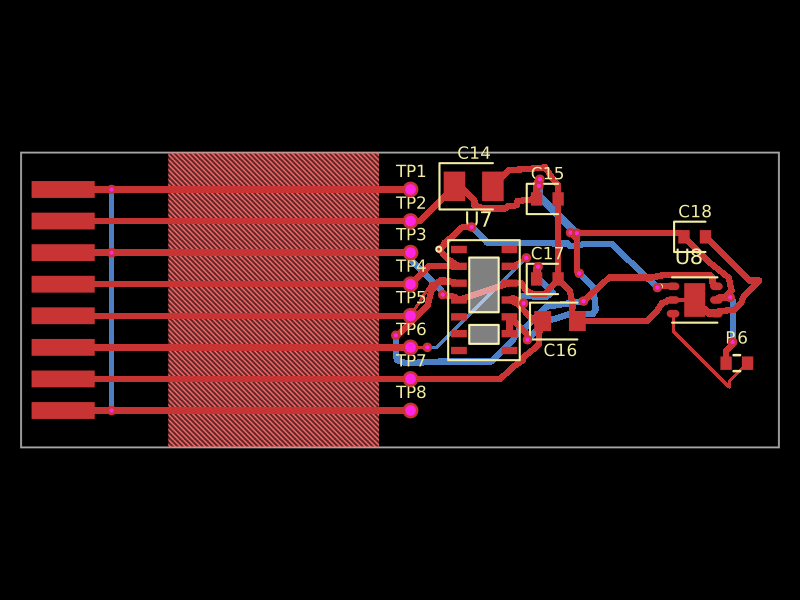 More from this authormohan-bee/fitness-band-sensor-flexA flexible dual-sensor PCB integrating a MAX30102 optical PPG/heart-rate sensor and TMP117 digital skin-temperature sensor, with I²C, power regulation, decoupling capacitors, interrupt pull-up, flex-tail connector, test points, and mechanical stiffeners/bend support.
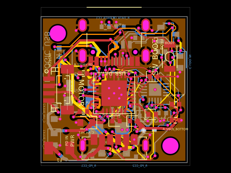 Discover something newShiboSoftwareDev/nema8-20mm-usbc-pd-controllerA 20×20 mm four-layer USB‑C PD stepper motor controller PCB using a CH32X035 MCU, TMC2209 driver, protected power inputs, USB data/boot interface, 3.3 V regulation, ESD/TVS protection, current-sense circuitry, and NEMA‑8 motor outputs.