mohan-bee/flight-controller-v2
A 64 mm STM32F405 flight-controller PCB with ICM-42688 IMU, SPI flash, USB-C/ESD, battery buck and 3.3 V regulation, four motor outputs, service I/O, and PETG standoff mounting hardware.
- Version
- 0.1.0
- License
- ISC
- Stars
- 0
tools/audit-manufacturing.py
import json, re, zipfile, runpy, math
from pathlib import Path
from shapely.geometry import Point, LineString, Polygon, box
from shapely.affinity import rotate, translate
from shapely.ops import unary_union
from shapely.validation import make_valid
from gerbonara import GerberFile, ExcellonFile
from gerbonara.utils import MM

env=runpy.run_path(str(Path(__file__).with_name('audit-copper.py')))
c=env['c'];root=env['root'];shapes=env['shapes'];errors=[]
release=root/'manufacturing/jlcpcb'
z=zipfile.ZipFile(release/'fabrication.zip')
def geometry(p):
    t=type(p).__name__
    if t=='Circle':return Point(p.x,p.y).buffer(p.r,resolution=96)
    if t=='Rectangle':
        return translate(rotate(box(-p.w/2,-p.h/2,p.w/2,p.h/2),math.degrees(p.rotation),origin=(0,0)),p.x,p.y)
    if t=='Line':return LineString([(p.x1,p.y1),(p.x2,p.y2)]).buffer(p.width/2,resolution=96)
    if t=='ArcPoly':
        assert not any(p.arc_centers or []),'Unexpected curved Gerber region'
        return make_valid(Polygon(p.outline))
    raise AssertionError(t)
layers={}
for name in z.namelist():
    if not name.endswith('.gbr'):continue
    parsed=GerberFile.from_string(z.read(name).decode(),filename=name)
    geom=Polygon();positives=[]
    for o in parsed.objects:
        for p in o.to_primitives():
            g=geometry(p)
            if p.polarity_dark:positives.append(g)
            else:
                geom=unary_union([geom,*positives]).difference(g);positives=[]
    layers[name]=(parsed,unary_union([geom,*positives]))
board=next(x for x in c if x['type']=='pcb_board')
outline=Polygon([(p['x'],p['y']) for p in board['outline']])
edge_min=100
for name in ['F_Cu.gbr','In1_Cu.gbr','In2_Cu.gbr','B_Cu.gbr']:
    geom=layers[name][1]
    if not outline.covers(geom):errors.append([name,'Copper outside board'])
    edge_min=min(edge_min,outline.boundary.distance(geom))
    if outline.boundary.distance(geom)<.499:errors.append([name,'Project 0.5 mm copper-edge clearance'])
# Check the final Gerber copper against the source geometry, including plane holes.
agreement={}
for layer,name in [('top','F_Cu.gbr'),('inner1','In1_Cu.gbr'),('inner2','In2_Cu.gbr'),('bottom','B_Cu.gbr')]:
    expected=[s['geom'] for s in shapes if layer in s['layers']]
    for p in (x for x in c if x['type']=='pcb_copper_pour' and x['layer']==layer):
        b=p['brep_shape'];expected.append(make_valid(Polygon([(v['x'],v['y']) for v in b['outer_ring']['vertices']], [[(v['x'],v['y']) for v in r['vertices']] for r in b['inner_rings']])))
    expected=unary_union(expected);actual=layers[name][1]
    missing=expected.difference(actual.buffer(.001)).area
    added=actual.difference(expected.buffer(.001)).area
    agreement[layer]=dict(missing_mm2=missing,added_mm2=added)
    if missing>1e-6 or added>1e-6:errors.append([name,'Circuit JSON / Gerber mismatch',missing,added])
# G85 is canonical Excellon, but gerbonara does not implement it. Interpret each
# one-block G85 as a routed slot in memory for independent drill geometry parsing.
drills=[];counts={}
for name,plated in [('drill-L1-L4.drl',True),('drill_npth.drl',False)]:
    text=z.read(name).decode();converted=[];slots=0
    for line in text.splitlines():
        if 'G85' in line:
            match=re.fullmatch(r'(X[-\d.]+Y[-\d.]+)G85(X[-\d.]+Y[-\d.]+)',line)
            assert match,line
            converted.extend(['G00'+match[1],'M15','G01'+match[2],'M16','G05']);slots+=1
        else:converted.append(line)
    parsed=ExcellonFile.from_string('\n'.join(converted),filename=name,plated=plated)
    counts[name]=dict(round_holes=len(list(parsed.drills())),slots=slots)
    for o in parsed.objects:
        drills.append(dict(geom=unary_union([geometry(p) for p in o.to_primitives(unit=MM)]),plated=plated,diameter=o.aperture.diameter))
assert counts['drill-L1-L4.drl']==dict(round_holes=sum(x['type']=='pcb_via' or (x['type']=='pcb_plated_hole' and x['shape'] in ['circle','circular_hole_with_rect_pad']) for x in c),slots=4),counts
assert counts['drill_npth.drl']==dict(round_holes=10,slots=0),counts
holegap=100
for i,a in enumerate(drills):
    for b in drills[i+1:]:
        gap=a['geom'].distance(b['geom']);holegap=min(holegap,gap)
        minimum=.25 if a['diameter']==b['diameter']==.25 else .45
        if gap+.001<minimum:errors.append(['Drill spacing',gap,minimum])
npthgap=min(d['geom'].distance(layers[name][1]) for d in drills if not d['plated'] for name in ['F_Cu.gbr','In1_Cu.gbr','In2_Cu.gbr','B_Cu.gbr'])
if npthgap<.199:errors.append(['NPTH to copper',npthgap])
via_ring=min((x['outer_diameter']-x['hole_diameter'])/2 for x in c if x['type']=='pcb_via')
pth_ring=min((x['outer_diameter']-x['hole_diameter'])/2 if x['shape']=='circle' else (min(x['rect_pad_width'],x['rect_pad_height'])-x['hole_diameter'])/2 if x['shape']=='circular_hole_with_rect_pad' else min(x['outer_width']-x['hole_width'],x['outer_height']-x['hole_height'])/2 for x in c if x['type']=='pcb_plated_hole')
if via_ring<.075 or pth_ring<.2-1e-9:errors.append(['Annular rings',via_ring,pth_ring])
mask=layers['F_Mask.gbr'][1];paste=layers['F_Paste.gbr'][1]
if paste.difference(mask.buffer(.001)).area>1e-6:
    errors.append(['Paste outside mask openings'])
pad_shapes={s['id']:s['geom'] for s in shapes if s['kind']=='pad'}
for p in (x for x in c if x['type']=='pcb_smtpad' and x.get('pcb_port_id')):
    if not mask.buffer(.001).covers(pad_shapes[p['pcb_smtpad_id']]):
        errors.append(['Top solder land not exposed',p['pcb_smtpad_id']])
for x,y in [(-30,0),(30,-24),(30,0)]:
    disk=Point(x,y).buffer(.999,resolution=96)
    if not mask.covers(disk):errors.append(['Fiducial mask',x,y])
    if paste.intersects(disk):errors.append(['Fiducial paste',x,y])
if not layers['B_Paste.gbr'][1].is_empty:errors.append(['Unexpected bottom paste'])
unpopulated={x['pcb_component_id'] for x in c if x['type']=='pcb_component' and x.get('do_not_place')}
for p in (x for x in c if x['type']=='pcb_smtpad' and x.get('pcb_component_id') in unpopulated):
    if paste.intersects(Point(p['x'],p['y'])):errors.append(['Bare pad has paste',p['pcb_smtpad_id']])
silk=layers['F_SilkScreen.gbr']
silk_gap=silk[1].distance(mask)
silk_width=min(p.width for o in silk[0].objects for p in o.to_primitives())
if silk_gap<.149 or silk_width<.149:errors.append(['Silkscreen rules',silk_gap,silk_width])
(release/'gerber-top-copper.svg').write_text(str(layers['F_Cu.gbr'][0].to_svg(fg='#e8bc6c',bg='#102019',force_bounds=((-30,-30),(30,30)))))
report=dict(status='pass' if not errors else 'fail',errors=errors,copper_edge_min_mm=edge_min,drill_counts=counts,drill_edge_gap_min_mm=holegap,npth_copper_gap_min_mm=npthgap,via_annular_ring_mm=via_ring,usb_slot_annular_ring_min_mm=pth_ring,silkscreen_mask_gap_mm=silk_gap,silkscreen_line_width_mm=silk_width,gerber_circuit_geometry_agreement=agreement,fiducials=3,top_assembly_only=True,scope='Independent Gerbonara parser and Shapely geometry audit of final tscircuit CAM. G85 slots interpreted as equivalent routed slots in memory. Not a manufacturer CAM approval or electrical/thermal qualification.')
(root/'validation/release/manufacturing-audit.json').write_text(json.dumps(report,indent=2)+'\n')
print(json.dumps(report,indent=2))
assert not errors
Related Packages
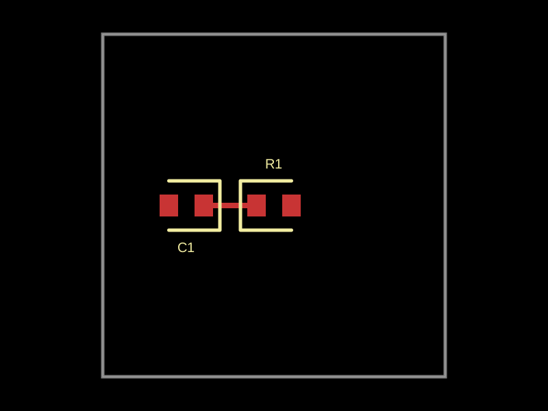 More from this authormohan-bee/repro-2This code defines a 10x10mm circuit board featuring a 1kΩ resistor and a 1000pF capacitor connected via 0402 footprint components.
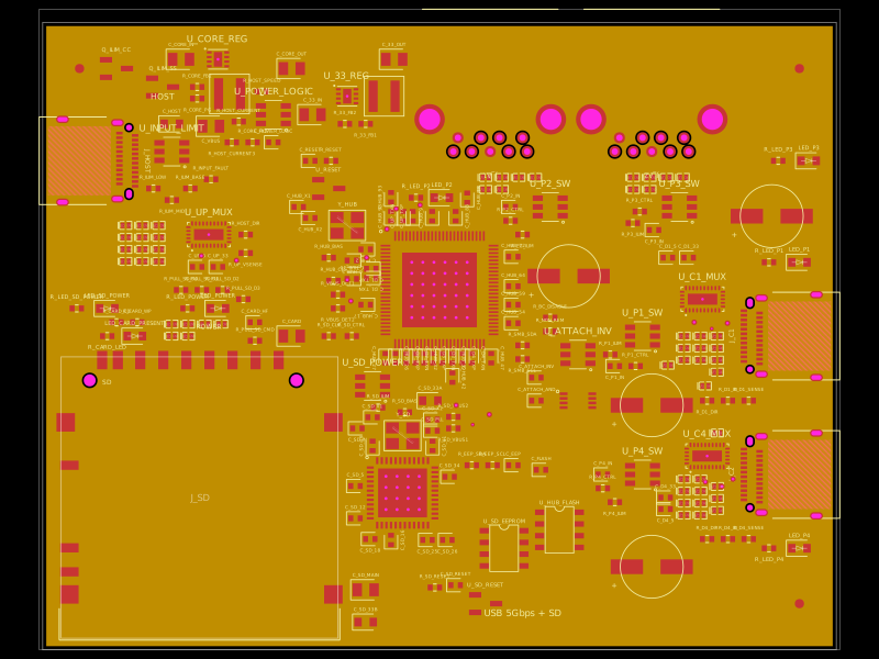 Similar packagegokul/usb3-sd-hubEngineering draft: four-layer, computer-powered USB 3 hub with one USB-C host socket, two USB-C and two USB-A accessory sockets, and a full-size SD slot. Board and three schematic previews are available. Routing and production checks are incomplete; not fabrication ready.
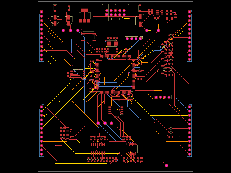 Discover something newhrithik18k/punck-tscircuit-recreationA four-layer Eurorack drum/sampler controller PCB built around an STM32H743, dual QSPI flash, PCM5100 stereo DAC, TL074 analog audio circuitry, input clamps, 12V-to-3.3V power regulation, MIDI/USB/SWD connectors, controls, LEDs, and trigger/audio I/O.