mohan-bee/flight-controller-v2
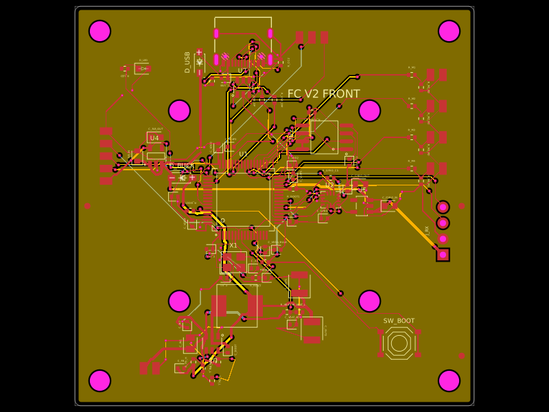
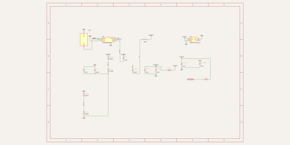
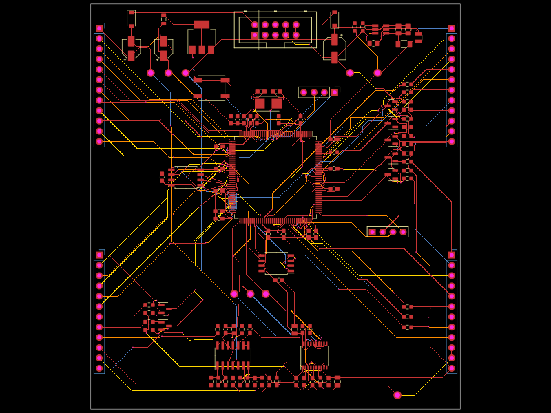
A 64 mm STM32F405 flight-controller PCB with ICM-42688 IMU, SPI flash, USB-C/ESD, battery buck and 3.3 V regulation, four motor outputs, service I/O, and PETG standoff mounting hardware.
- Version
- 0.1.0
- License
- ISC
- Stars
- 0
index.circuit.tsx
PCB
Schematic
import { UsbCFootprint } from "./imports/UsbCFootprint";
import { reviewedRouting } from "./routing/reviewed-routing";
import { STM32F405RGT6 } from "./imports/STM32F405RGT6";
import { ICM_42688_P } from "./imports/ICM_42688_P";
import { TPS54302DDCR } from "./imports/TPS54302DDCR";
import { AP2112K_3_3TRG1 } from "./imports/AP2112K_3_3TRG1";
import { LP5907MFX_3_3_NOPB } from "./imports/LP5907MFX_3_3_NOPB";
import { W25Q128JVSIQ } from "./imports/W25Q128JVSIQ";
import { USBLC6_2SC6 } from "./imports/USBLC6_2SC6";
import { TAXM8M4RDBCCT2T } from "./imports/TAXM8M4RDBCCT2T";
import { B5819W_SL } from "./imports/B5819W_SL";
import { IHLP2525CZER100M01 } from "./imports/IHLP2525CZER100M01";
import { TS_1187A_B_A_B } from "./imports/TS_1187A_B_A_B";
import type { BoardProps } from "@tscircuit/props";
export default function FlightController({
routingDisabled = false,
...boardProps
}: Pick<BoardProps, "routingDisabled" | "name" | "mountedTo"> = {}) {
return (
<board
{...boardProps}
routingDisabled={routingDisabled}
width="64mm"
height="64mm"
layers={4}
thickness="1.6mm"
borderRadius="1mm"
schTraceAutoLabelEnabled
autorouter={{ preset: "auto", traceClearance: "0.3mm", allowViaInPad: false }}
minTraceWidth="0.15mm"
minViaHoleEdgeToViaHoleEdgeClearance="0.25mm"
minTraceToPadEdgeClearance="0.2mm"
minViaEdgeToPadEdgeClearance="0.2mm"
minBoardEdgeClearance="0.5mm"
minTraceToHoleEdgeClearance="0.3mm"
minViaHoleDiameter="0.25mm"
minViaPadDiameter="0.5mm"
>
<autoroutingphase
name="flight-controller"
phaseIndex={0}
algorithmFn={reviewedRouting}
autorouter={{ preset: "auto", traceClearance: "0.3mm", allowViaInPad: false }}
/>
<schematicsheet name="sheet_power" displayName="01 - Power supplies" sheetIndex={0} />
<schematicsheet name="sheet_mcu" displayName="02 - STM32 controller" sheetIndex={1} />
<schematicsheet name="sheet_support" displayName="03 - MCU power, clock and reset" sheetIndex={2} />
<schematicsheet name="sheet_gyro" displayName="04 - IMU and filtered supply" sheetIndex={3} />
<schematicsheet name="sheet_flash" displayName="05 - SPI flash" sheetIndex={4} />
<schematicsheet name="sheet_usb" displayName="06 - USB connector and protection" sheetIndex={5} />
<schematicsheet name="sheet_io" displayName="07 - Receiver, service IO and monitoring" sheetIndex={6} />
<schematicsheet name="sheet_motors" displayName="08 - Four motor outputs" sheetIndex={7} />
<schematicsection name="Motors" schSheetName="sheet_motors" />
<schematicsection name="Power" schSheetName="sheet_power" />
{/* Keep copper clear of both USB locating holes on every copper layer. */}
<keepout
shape="circle"
pcbX={-2.110115}
pcbY={23.94507445}
radius="0.65mm"
layers={["top", "inner1", "inner2", "bottom"]}
allowPlacements
/>
<keepout
shape="circle"
pcbX={-7.890139}
pcbY={23.94507445}
radius="0.65mm"
layers={["top", "inner1", "inner2", "bottom"]}
allowPlacements
/>
<schematicsection name="MCU" schSheetName="sheet_mcu" />
<schematicsection name="Gyro" schSheetName="sheet_gyro" />
<schematicsection name="USB" schSheetName="sheet_usb" />
<schematicsection name="IO" schSheetName="sheet_io" />
<schematicsection name="Flash" schSheetName="sheet_flash" />
<schematicsection name="Support" schSheetName="sheet_support" />
<STM32F405RGT6
name="U1"
pcbX={-5}
pcbY={1}
schSectionName="MCU"
schSheetName="sheet_mcu"
schX={0}
schY={1}
schWidth={4.525}
schHeight={10.4}
schPinStyle={Object.fromEntries(
Array.from({ length: 64 }, (_, index) => [
`pin${index + 1}`,
{ marginBottom: index === 47 || index === 48 ? 0.4 : 0.1 },
]),
)}
/>
<trace
from=".U1 > .pin1"
to="net.V3V3"
schDisplayLabel="V3V3"
width={0.25}
/>
<trace
name="OSC_IN_MCU"
routingPhaseIndex={0}
from=".U1 > .pin5"
to=".X1 > .pin1"
schDisplayLabel="OSC_IN"
width={0.15}
pcbPath={[
{ x: -1.75006, y: -7.1 },
{ x: -4.3, y: -7.1 },
{ x: -4.3, y: -10.850011 },
".X1 > .pin1",
]}
/>
<trace
name="OSC_OUT_MCU"
routingPhaseIndex={0}
from=".U1 > .pin6"
to=".X1 > .pin3"
schDisplayLabel="OSC_OUT"
width={0.15}
pcbPath={[
{ x: -1.249934, y: -7.1 },
{ x: -0.399926, y: -7.95 },
".X1 > .pin3",
]}
/>
<trace
from=".U1 > .pin7"
to="net.NRST"
schDisplayLabel="NRST"
width={0.15}
/>
<trace
from=".U1 > .pin8"
to="net.VBAT_ADC"
schDisplayLabel="VBAT_ADC"
width={0.15}
/>
<trace
from=".U1 > .pin12"
to="net.GND"
schDisplayLabel="GND"
width={0.2}
/>
<trace
from=".U1 > .pin13"
to="net.VDDA"
schDisplayLabel="VDDA"
width={0.2}
/>
<trace
from=".U1 > .pin18"
to="net.GND"
schDisplayLabel="GND"
width={0.2}
/>
<trace
from=".U1 > .pin19"
to="net.V3V3"
schDisplayLabel="V3V3"
width={0.25}
/>
<trace
from=".U1 > .pin20"
to="net.GYRO_CS"
schDisplayLabel="GYRO_CS"
width={0.15}
/>
<trace
from=".U1 > .pin21"
to="net.GYRO_SCK"
schDisplayLabel="GYRO_SCK"
width={0.15}
/>
<trace
from=".U1 > .pin22"
to="net.GYRO_MISO"
schDisplayLabel="GYRO_MISO"
width={0.15}
/>
<trace
from=".U1 > .pin23"
to="net.GYRO_MOSI"
schDisplayLabel="GYRO_MOSI"
width={0.15}
/>
<trace
from=".U1 > .pin24"
to="net.GYRO_INT"
schDisplayLabel="GYRO_INT"
width={0.15}
/>
<trace
from=".U1 > .pin28"
to="net.BOOT1"
schDisplayLabel="BOOT1"
width={0.15}
/>
<trace
from=".U1 > .pin29"
to="net.RX_TX"
schDisplayLabel="RX_TX"
width={0.15}
/>
<trace
from=".U1 > .pin30"
to="net.RX_RX"
schDisplayLabel="RX_RX"
width={0.15}
/>
<trace
from=".U1 > .pin31"
to="net.VCAP1"
schDisplayLabel="VCAP1"
width={0.15}
/>
<trace
from=".U1 > .pin32"
to="net.V3V3"
schDisplayLabel="V3V3"
width={0.25}
/>
<trace
from=".U1 > .pin33"
to="net.FLASH_CS"
schDisplayLabel="FLASH_CS"
width={0.15}
/>
<trace
from=".U1 > .pin34"
to="net.FLASH_SCK"
schDisplayLabel="FLASH_SCK"
width={0.15}
/>
<trace
from=".U1 > .pin35"
to="net.FLASH_MISO"
schDisplayLabel="FLASH_MISO"
width={0.15}
/>
<trace
from=".U1 > .pin36"
to="net.FLASH_MOSI"
schDisplayLabel="FLASH_MOSI"
width={0.15}
/>
<trace
from=".U1 > .pin37"
to="net.M1"
schDisplayLabel="M1"
width={0.15}
/>
<trace
from=".U1 > .pin38"
to="net.M2"
schDisplayLabel="M2"
width={0.15}
/>
<trace
from=".U1 > .pin39"
to="net.M3"
schDisplayLabel="M3"
width={0.15}
/>
<trace
from=".U1 > .pin40"
to="net.M4"
schDisplayLabel="M4"
width={0.15}
/>
<trace
from=".U1 > .pin42"
to="net.USB_VBUS"
schDisplayLabel="USB_VBUS"
width={0.15}
/>
<trace
from=".U1 > .pin44"
to="net.USB_DM_MCU"
schDisplayLabel="USB_DM_MCU"
width={0.15}
/>
<trace
from=".U1 > .pin45"
to="net.USB_DP_MCU"
schDisplayLabel="USB_DP_MCU"
width={0.15}
/>
<trace
from=".U1 > .pin46"
to="net.SWDIO"
schDisplayLabel="SWDIO"
width={0.15}
/>
<trace
from=".U1 > .pin47"
to="net.VCAP2"
schDisplayLabel="VCAP2"
width={0.15}
/>
<trace
from=".U1 > .pin48"
to="net.V3V3"
schDisplayLabel="V3V3"
width={0.25}
/>
<trace
from=".U1 > .pin49"
to="net.SWCLK"
schDisplayLabel="SWCLK"
width={0.15}
/>
<trace
from=".U1 > .pin51"
to="net.UART4_TX"
schDisplayLabel="UART4_TX"
width={0.15}
/>
<trace
from=".U1 > .pin52"
to="net.UART4_RX"
schDisplayLabel="UART4_RX"
width={0.15}
/>
<trace
from=".U1 > .pin58"
to="net.LED"
schDisplayLabel="LED"
width={0.15}
/>
<trace
from=".U1 > .pin60"
to="net.BOOT0"
schDisplayLabel="BOOT0"
width={0.15}
/>
<trace
from=".U1 > .pin63"
to="net.GND"
schDisplayLabel="GND"
width={0.2}
/>
<trace
from=".U1 > .pin64"
to="net.V3V3"
schDisplayLabel="V3V3"
width={0.25}
/>
<ICM_42688_P
name="U2"
pcbX={9.0}
pcbY={1}
schSectionName="Gyro"
schSheetName="sheet_gyro"
schX={3}
schY={3}
schWidth={2.34}
schHeight={1.6}
/>
<trace
from=".U2 > .pin1"
to="net.GYRO_MISO"
schDisplayLabel="GYRO_MISO"
width={0.15}
/>
<trace
from=".U2 > .pin2"
to="net.GND"
schDisplayLabel="GND"
width={0.2}
/>
<trace
from=".U2 > .pin3"
to="net.GND"
schDisplayLabel="GND"
width={0.2}
/>
<trace
from=".U2 > .pin4"
to="net.GYRO_INT"
schDisplayLabel="GYRO_INT"
width={0.15}
/>
<trace
from=".U2 > .pin5"
to="net.GYRO_3V3"
schDisplayLabel="GYRO_3V3"
width={0.2}
/>
<trace
from=".U2 > .pin6"
to="net.GND"
schDisplayLabel="GND"
width={0.2}
/>
<trace
from=".U2 > .pin7"
to="net.GND"
schDisplayLabel="GND"
width={0.2}
/>
<trace
from=".U2 > .pin8"
to="net.GYRO_3V3"
schDisplayLabel="GYRO_3V3"
width={0.2}
/>
<trace
from=".U2 > .pin9"
to="net.GND"
schDisplayLabel="GND"
width={0.2}
/>
<trace
from=".U2 > .pin10"
to="net.GND"
schDisplayLabel="GND"
width={0.2}
/>
<trace
from=".U2 > .pin11"
to="net.GND"
schDisplayLabel="GND"
width={0.2}
/>
<trace
from=".U2 > .pin12"
to="net.GYRO_CS"
schDisplayLabel="GYRO_CS"
width={0.15}
/>
<trace
from=".U2 > .pin13"
to="net.GYRO_SCK"
schDisplayLabel="GYRO_SCK"
width={0.15}
/>
<trace
from=".U2 > .pin14"
to="net.GYRO_MOSI"
schDisplayLabel="GYRO_MOSI"
width={0.15}
/>
<TPS54302DDCR
name="U3"
pcbX={-10}
pcbY={-22.0}
schSectionName="Power"
schSheetName="sheet_power"
schX={-7}
schY={5}
schWidth={1.865}
schHeight={0.8}
layer="top"
pcbRotation={180}
/>
<trace
from=".U3 > .pin1"
to="net.GND"
schDisplayLabel="GND"
width={0.2}
/>
<trace from=".U3 > .pin2" to="net.SW" schDisplayLabel="SW" width={0.5} />
<trace
from=".U3 > .pin3"
to="net.VBAT"
schDisplayLabel="VBAT"
width={0.4}
/>
<trace
from=".U3 > .pin4"
to="net.BUCK_FB"
schDisplayLabel="BUCK_FB"
width={0.15}
/>
<trace
from=".U3 > .pin5"
to="net.BUCK_EN"
schDisplayLabel="BUCK_EN"
width={0.15}
/>
<trace
from=".U3 > .pin6"
to="net.BOOT"
schDisplayLabel="BOOT"
width={0.15}
/>
<AP2112K_3_3TRG1
name="U4"
pcbX={-19}
pcbY={8}
schSectionName="Power"
schSheetName="sheet_power"
schX={7}
schY={5}
/>
<trace
from=".U4 > .pin1"
to="net.V5_SYS"
schDisplayLabel="V5_SYS"
width={0.4}
/>
<trace
from=".U4 > .pin2"
to="net.GND"
schDisplayLabel="GND"
width={0.2}
/>
<trace
from=".U4 > .pin3"
to="net.V5_SYS"
schDisplayLabel="V5_SYS"
width={0.4}
/>
<trace
from=".U4 > .pin5"
to="net.V3V3"
schDisplayLabel="V3V3"
width={0.25}
/>
<LP5907MFX_3_3_NOPB
name="U5"
pcbX={14.0}
pcbY={0}
schSectionName="Gyro"
schSheetName="sheet_gyro"
schX={-5}
schY={3}
layer="top"
/>
<trace
from=".U5 > .pin1"
to="net.V5_SYS"
schDisplayLabel="V5_SYS"
width={0.4}
/>
<trace
from=".U5 > .pin2"
to="net.GND"
schDisplayLabel="GND"
width={0.2}
/>
<trace
from=".U5 > .pin3"
to="net.V5_SYS"
routingPhaseIndex={0}
schDisplayLabel="V5_SYS"
width={0.4}
/>
<trace
from=".U5 > .pin5"
to="net.GYRO_3V3"
schDisplayLabel="GYRO_3V3"
width={0.2}
/>
<W25Q128JVSIQ
name="U6"
pcbX={8}
pcbY={11}
schSectionName="Flash"
schSheetName="sheet_flash"
schX={0}
schY={3}
schWidth={1.865}
schHeight={1}
pcbRotation={90}
/>
<trace
from=".U6 > .pin1"
to="net.FLASH_CS"
schDisplayLabel="FLASH_CS"
width={0.15}
/>
<trace
from=".U6 > .pin2"
to="net.FLASH_MISO"
schDisplayLabel="FLASH_MISO"
width={0.15}
/>
<trace
from=".U6 > .pin3"
to="net.V3V3"
schDisplayLabel="V3V3"
width={0.25}
/>
<trace
from=".U6 > .pin4"
to="net.GND"
schDisplayLabel="GND"
width={0.2}
/>
<trace
from=".U6 > .pin5"
to="net.FLASH_MOSI"
schDisplayLabel="FLASH_MOSI"
width={0.15}
/>
<trace
from=".U6 > .pin6"
to="net.FLASH_SCK"
schDisplayLabel="FLASH_SCK"
width={0.15}
/>
<trace
from=".U6 > .pin7"
to="net.V3V3"
schDisplayLabel="V3V3"
width={0.25}
/>
<trace
from=".U6 > .pin8"
to="net.V3V3"
schDisplayLabel="V3V3"
width={0.25}
/>
<connector
name="J_USB"
pcbX={-5.0}
pcbY={25.0}
schSectionName="USB"
schSheetName="sheet_usb"
schX={0}
schY={4}
standard="usb_c"
footprint={<UsbCFootprint />}
manufacturerPartNumber="TYPE-C 16PIN 2MD(073)"
supplierPartNumbers={{ jlcpcb: ["C2765186"] }}
schWidth={1.6}
schHeight={3.641}
pcbRotation={180}
/>
<trace
from=".J_USB > .GND1"
to="net.GND"
schDisplayLabel="GND"
width={0.2}
/>
<trace
from=".J_USB > .GND2"
to="net.GND"
schDisplayLabel="GND"
width={0.2}
/>
<trace
from=".J_USB > .VBUS1"
to="net.USB_VBUS"
schDisplayLabel="USB_VBUS"
width={0.15}
/>
<trace
from=".J_USB > .VBUS2"
to="net.USB_VBUS"
schDisplayLabel="USB_VBUS"
width={0.15}
/>
<trace
from=".J_USB > .CC1"
to="net.CC1"
schDisplayLabel="CC1"
width={0.15}
/>
<trace
from=".J_USB > .CC2"
to="net.CC2"
schDisplayLabel="CC2"
width={0.15}
/>
<trace
from=".J_USB > .DP1"
to="net.USB_DP"
schDisplayLabel="USB_DP"
width={0.15}
/>
<trace
from=".J_USB > .DP2"
to="net.USB_DP"
schDisplayLabel="USB_DP"
width={0.15}
/>
<trace
from=".J_USB > .DM1"
to="net.USB_DM"
schDisplayLabel="USB_DM"
width={0.15}
/>
<trace
from=".J_USB > .DM2"
to="net.USB_DM"
schDisplayLabel="USB_DM"
width={0.15}
/>
<trace
from=".J_USB > .SHELL1"
to="net.GND"
schDisplayLabel="GND"
width={0.2}
/>
<trace
from=".J_USB > .SHELL2"
to="net.GND"
schDisplayLabel="GND"
width={0.2}
/>
{/* The builtin footprint creates separate ports for the repeated shell pins. */}
<trace
from=".J_USB > .pin13_internal_1"
to="net.GND"
schDisplayLabel="GND"
width={0.2}
/>
<trace
from=".J_USB > .pin14_internal_1"
to="net.GND"
schDisplayLabel="GND"
width={0.2}
/>
<USBLC6_2SC6
name="U7"
pcbX={-5.0}
pcbY={19.0}
schSectionName="USB"
schSheetName="sheet_usb"
schX={-5}
schY={-2}
/>
<trace
from=".U7 > .pin1"
to="net.USB_DM"
schDisplayLabel="USB_DM"
width={0.15}
/>
<trace
from=".U7 > .pin2"
to="net.GND"
schDisplayLabel="GND"
width={0.2}
/>
<trace
from=".U7 > .pin3"
to="net.USB_DP"
schDisplayLabel="USB_DP"
width={0.15}
/>
<trace
from=".U7 > .pin4"
to="net.USB_DP_ESD"
schDisplayLabel="USB_DP_ESD"
width={0.15}
/>
<trace
from=".U7 > .pin5"
to="net.USB_VBUS"
schDisplayLabel="USB_VBUS"
width={0.15}
/>
<trace
from=".U7 > .pin6"
to="net.USB_DM_ESD"
schDisplayLabel="USB_DM_ESD"
width={0.15}
/>
<resistor
name="R_USB_DP"
pcbX={-2.0}
pcbY={17.0}
schSectionName="USB"
schSheetName="sheet_usb"
schX={3}
schY={-2}
resistance="22"
footprint="0402"
pcbRotation={270}
schRotation={-90}
supplierPartNumbers={{ jlcpcb: ["C25092"] }}
/>
<trace
from=".R_USB_DP > .pin1"
to="net.USB_DP_ESD"
schDisplayLabel="USB_DP_ESD"
width={0.15}
/>
<trace
from=".R_USB_DP > .pin2"
to="net.USB_DP_MCU"
schDisplayLabel="USB_DP_MCU"
width={0.15}
/>
<resistor
name="R_USB_DM"
pcbX={0.0}
pcbY={17.0}
schSectionName="USB"
schSheetName="sheet_usb"
schX={8}
schY={-2}
resistance="22"
footprint="0402"
pcbRotation={270}
schRotation={-90}
supplierPartNumbers={{ jlcpcb: ["C25092"] }}
/>
<trace
from=".R_USB_DM > .pin1"
to="net.USB_DM_ESD"
schDisplayLabel="USB_DM_ESD"
width={0.15}
/>
<trace
from=".R_USB_DM > .pin2"
to="net.USB_DM_MCU"
schDisplayLabel="USB_DM_MCU"
width={0.15}
/>
<resistor
name="R_CC1"
pcbX={-10.0}
pcbY={20.0}
schSectionName="USB"
schSheetName="sheet_usb"
schX={-5}
schY={-7}
resistance="5.1k"
footprint="0402"
pcbRotation={270}
schRotation={-90}
supplierPartNumbers={{ jlcpcb: ["C25905"] }}
/>
<trace
from=".R_CC1 > .pin1"
to="net.CC1"
schDisplayLabel="CC1"
width={0.15}
/>
<trace
from=".R_CC1 > .pin2"
to="net.GND"
schDisplayLabel="GND"
width={0.2}
/>
<resistor
name="R_CC2"
pcbX={1.0}
pcbY={23.0}
schSectionName="USB"
schSheetName="sheet_usb"
schX={0}
schY={-7}
resistance="5.1k"
footprint="0402"
pcbRotation={90}
schRotation={-90}
supplierPartNumbers={{ jlcpcb: ["C25905"] }}
/>
<trace
from=".R_CC2 > .pin1"
to="net.CC2"
schDisplayLabel="CC2"
width={0.15}
/>
<trace
from=".R_CC2 > .pin2"
to="net.GND"
schDisplayLabel="GND"
width={0.2}
/>
<capacitor
name="C_USB"
pcbX={-8.0}
pcbY={20.5}
schSectionName="USB"
schSheetName="sheet_usb"
schX={5}
schY={-7}
capacitance="100nF"
footprint="0402"
pcbRotation={180}
schRotation={-90}
maxVoltageRating="10V"
supplierPartNumbers={{ jlcpcb: ["C1525"] }}
/>
<trace
from=".C_USB > .pin1"
to="net.USB_VBUS"
schDisplayLabel="USB_VBUS"
width={0.15}
/>
<trace
from=".C_USB > .pin2"
to="net.GND"
schDisplayLabel="GND"
width={0.2}
/>
<B5819W_SL
name="D_USB"
pcbX={-12.0}
pcbY={23.0}
schSectionName="Power"
schSheetName="sheet_power"
schX={9}
schY={-1.5}
pcbRotation={90}
/>
<trace
from=".D_USB > .pin1"
to="net.V5_SYS"
schDisplayLabel="V5_SYS"
width={0.4}
/>
<trace
from=".D_USB > .pin2"
to="net.USB_VBUS"
schDisplayLabel="USB_VBUS"
width={0.15}
/>
<B5819W_SL
name="D_BUCK"
pcbX={-14.8}
pcbY={4.5}
schSectionName="Power"
schSheetName="sheet_power"
schX={3}
schY={0}
layer="top"
/>
<trace
from=".D_BUCK > .pin1"
to="net.V5_SYS"
schDisplayLabel="V5_SYS"
width={0.4}
/>
<trace
from=".D_BUCK > .pin2"
to="net.V5_BUCK"
schDisplayLabel="V5_BUCK"
width={0.4}
/>
<chip
name="J_BAT"
doNotPlace
pcbX={-20}
pcbY={-26}
schSectionName="Power"
schSheetName="sheet_power"
schX={-11}
schY={5}
pinLabels={{ pin1: ["VBAT"], pin2: ["GND"] }}
footprint={
<footprint insertionDirection="from_above">
<smtpad
portHints={["pin1"]}
pcbX={-1}
pcbY={0}
width="1.2mm"
height="2mm"
shape="rect"
schPinArrangement={{ topSide: [1], bottomSide: [2] }}
schWidth={1.2}
schHeight={2}
/>
<smtpad
portHints={["pin2"]}
pcbX={1}
pcbY={0}
width="1.2mm"
height="2mm"
shape="rect"
schPinArrangement={{ topSide: [1], bottomSide: [2] }}
schWidth={1.2}
schHeight={2}
/>
</footprint>
}
pcbRotation={0}
schPinArrangement={{ topSide: [1], bottomSide: [2] }}
schWidth={1.2}
schHeight={2}
/>
<trace
from=".J_BAT > .pin1"
to="net.VBAT"
schDisplayLabel="VBAT"
width={0.4}
/>
<trace
from=".J_BAT > .pin2"
to="net.GND"
schDisplayLabel="GND"
width={0.2}
/>
<IHLP2525CZER100M01
name="L1"
pcbX={-6}
pcbY={-16}
schSectionName="Power"
schSheetName="sheet_power"
schX={-1}
schY={5}
layer="top"
pcbRotation={0}
/>
<trace from=".L1 > .pin1" to="net.SW" schDisplayLabel="SW" width={0.5} />
<trace
from=".L1 > .pin2"
to="net.V5_BUCK"
schDisplayLabel="V5_BUCK"
width={0.4}
/>
<capacitor
name="C_IN1"
pcbX={-13.5}
pcbY={-22.0}
schSectionName="Power"
schSheetName="sheet_power"
schX={-11}
schY={0}
capacitance="10uF"
footprint="0805"
pcbRotation={90}
layer="top"
schRotation={-90}
maxVoltageRating="25V"
supplierPartNumbers={{ jlcpcb: ["C15850"] }}
/>
<trace
from=".C_IN1 > .pin1"
to="net.VBAT"
schDisplayLabel="VBAT"
width={0.4}
/>
<trace
from=".C_IN1 > .pin2"
to="net.GND"
schDisplayLabel="GND"
width={0.2}
/>
<capacitor
name="C_IN2"
pcbX={-14}
pcbY={-19.0}
schSectionName="Power"
schSheetName="sheet_power"
schX={-9.2}
schY={0}
capacitance="100nF"
footprint="0402"
pcbRotation={90}
layer="top"
schRotation={-90}
maxVoltageRating="25V"
supplierPartNumbers={{ jlcpcb: ["C1525"] }}
/>
<trace
from=".C_IN2 > .pin1"
to="net.VBAT"
schDisplayLabel="VBAT"
width={0.4}
/>
<trace
from=".C_IN2 > .pin2"
to="net.GND"
schDisplayLabel="GND"
width={0.2}
/>
<capacitor
name="C_BOOT"
pcbX={-7.5}
pcbY={-23.0}
schSectionName="Power"
schSheetName="sheet_power"
schX={-3}
schY={0}
capacitance="100nF"
footprint="0402"
pcbRotation={90}
layer="top"
schRotation={-90}
maxVoltageRating="10V"
supplierPartNumbers={{ jlcpcb: ["C1525"] }}
/>
<trace
from=".C_BOOT > .pin1"
to="net.BOOT"
schDisplayLabel="BOOT"
width={0.15}
/>
<trace
from=".C_BOOT > .pin2"
to="net.SW"
schDisplayLabel="SW"
width={0.5}
/>
<capacitor
name="C_OUT1"
pcbX={4}
pcbY={-12.5}
schSectionName="Power"
schSheetName="sheet_power"
schX={-1}
schY={0}
capacitance="47uF"
footprint="1210"
pcbRotation={90}
layer="top"
schRotation={-90}
maxVoltageRating="16V"
supplierPartNumbers={{ jlcpcb: ["C77101"] }}
/>
<trace
from=".C_OUT1 > .pin1"
to="net.V5_BUCK"
schDisplayLabel="V5_BUCK"
width={0.4}
/>
<trace
from=".C_OUT1 > .pin2"
to="net.GND"
schDisplayLabel="GND"
width={0.2}
/>
<capacitor
name="C_OUT2"
pcbX={6}
pcbY={-20}
schSectionName="Power"
schSheetName="sheet_power"
schX={0.8}
schY={0}
capacitance="47uF"
footprint="1210"
pcbRotation={270}
layer="top"
schRotation={-90}
maxVoltageRating="16V"
supplierPartNumbers={{ jlcpcb: ["C77101"] }}
/>
<trace
from=".C_OUT2 > .pin1"
to="net.V5_BUCK"
schDisplayLabel="V5_BUCK"
width={0.4}
/>
<trace
from=".C_OUT2 > .pin2"
to="net.GND"
schDisplayLabel="GND"
width={0.2}
/>
<resistor
name="R_FB_H"
pcbX={-13}
pcbY={-25}
schSectionName="Power"
schSheetName="sheet_power"
schX={-7}
schY={2}
resistance="100k"
footprint="0402"
pcbRotation={90}
layer="top"
schRotation={-90}
supplierPartNumbers={{ jlcpcb: ["C25741"] }}
/>
<trace
from=".R_FB_H > .pin1"
to="net.V5_BUCK"
schDisplayLabel="V5_BUCK"
width={0.4}
/>
<trace
from=".R_FB_H > .pin2"
to="net.BUCK_FB"
schDisplayLabel="BUCK_FB"
width={0.15}
/>
<resistor
name="R_FB_L"
pcbX={-11.5}
pcbY={-26}
schSectionName="Power"
schSheetName="sheet_power"
schX={-7}
schY={0}
resistance="13.3k"
footprint="0402"
pcbRotation={270}
layer="top"
schRotation={-90}
supplierPartNumbers={{ jlcpcb: ["C2974007"] }}
/>
<trace
from=".R_FB_L > .pin1"
to="net.BUCK_FB"
schDisplayLabel="BUCK_FB"
width={0.15}
/>
<trace
from=".R_FB_L > .pin2"
to="net.GND"
schDisplayLabel="GND"
width={0.2}
/>
<capacitor
name="C_FB"
pcbX={-15}
pcbY={-26}
schSectionName="Power"
schSheetName="sheet_power"
schX={-4.5}
schY={2}
capacitance="75pF"
footprint="0402"
pcbRotation={0}
layer="top"
schRotation={-90}
maxVoltageRating="10V"
supplierPartNumbers={{ jlcpcb: ["C107010"] }}
/>
<trace
from=".C_FB > .pin1"
to="net.V5_BUCK"
schDisplayLabel="V5_BUCK"
width={0.4}
/>
<trace
from=".C_FB > .pin2"
to="net.BUCK_FB"
schDisplayLabel="BUCK_FB"
width={0.15}
/>
<resistor
name="R_EN_H"
pcbX={-9}
pcbY={-25}
schSectionName="Power"
schSheetName="sheet_power"
schX={-11}
schY={-4}
resistance="511k"
footprint="0402"
pcbRotation={90}
layer="top"
schRotation={-90}
supplierPartNumbers={{ jlcpcb: ["C5126239"] }}
/>
<trace
from=".R_EN_H > .pin1"
to="net.VBAT"
schDisplayLabel="VBAT"
width={0.4}
/>
<trace
from=".R_EN_H > .pin2"
to="net.BUCK_EN"
schDisplayLabel="BUCK_EN"
width={0.15}
/>
<resistor
name="R_EN_L"
pcbX={-10}
pcbY={-28}
schSectionName="Power"
schSheetName="sheet_power"
schX={-11}
schY={-7}
resistance="105k"
footprint="0402"
pcbRotation={270}
layer="top"
schRotation={-90}
supplierPartNumbers={{ jlcpcb: ["C2933067"] }}
/>
<trace
from=".R_EN_L > .pin1"
to="net.BUCK_EN"
schDisplayLabel="BUCK_EN"
width={0.15}
/>
<trace
from=".R_EN_L > .pin2"
to="net.GND"
schDisplayLabel="GND"
width={0.2}
/>
<capacitor
name="C_3V3_IN"
pcbX={-22}
pcbY={8}
schSectionName="Power"
schSheetName="sheet_power"
schX={5}
schY={1}
capacitance="4.7uF"
footprint="0603"
pcbRotation={90}
schRotation={-90}
maxVoltageRating="16V"
supplierPartNumbers={{ jlcpcb: ["C19666"] }}
/>
<trace
from=".C_3V3_IN > .pin1"
to="net.V5_SYS"
schDisplayLabel="V5_SYS"
width={0.4}
/>
<trace
from=".C_3V3_IN > .pin2"
to="net.GND"
schDisplayLabel="GND"
width={0.2}
/>
<capacitor
name="C_3V3_OUT"
pcbX={-19}
pcbY={11}
schSectionName="Power"
schSheetName="sheet_power"
schX={8}
schY={1}
capacitance="4.7uF"
footprint="0603"
pcbRotation={0}
schRotation={-90}
maxVoltageRating="16V"
supplierPartNumbers={{ jlcpcb: ["C19666"] }}
/>
<trace
from=".C_3V3_OUT > .pin1"
to="net.V3V3"
schDisplayLabel="V3V3"
width={0.25}
/>
<trace
from=".C_3V3_OUT > .pin2"
to="net.GND"
schDisplayLabel="GND"
width={0.2}
/>
<capacitor
name="C_GYRO_IN"
pcbX={18.5}
pcbY={0}
schSectionName="Gyro"
schSheetName="sheet_gyro"
schX={-9}
schY={3}
capacitance="4.7uF"
footprint="0603"
pcbRotation={0}
layer="top"
schRotation={-90}
maxVoltageRating="16V"
supplierPartNumbers={{ jlcpcb: ["C19666"] }}
/>
<trace
from=".C_GYRO_IN > .pin1"
to="net.V5_SYS"
schDisplayLabel="V5_SYS"
width={0.4}
/>
<trace
from=".C_GYRO_IN > .pin2"
to="net.GND"
schDisplayLabel="GND"
width={0.2}
/>
<capacitor
name="C_GYRO_OUT"
pcbX={13.8}
pcbY={3.5}
schSectionName="Gyro"
schSheetName="sheet_gyro"
schX={-6}
schY={-2}
capacitance="4.7uF"
footprint="0603"
pcbRotation={0}
schRotation={-90}
maxVoltageRating="16V"
supplierPartNumbers={{ jlcpcb: ["C19666"] }}
/>
<trace
from=".C_GYRO_OUT > .pin1"
to="net.GYRO_3V3"
schDisplayLabel="GYRO_3V3"
width={0.2}
/>
<trace
from=".C_GYRO_OUT > .pin2"
to="net.GND"
schDisplayLabel="GND"
width={0.2}
/>
<capacitor
name="C_GYRO_VDD"
pcbX={11.7}
pcbY={2.9}
schSectionName="Gyro"
schSheetName="sheet_gyro"
schX={-4.2}
schY={-2}
capacitance="100nF"
footprint="0402"
pcbRotation={90}
schRotation={-90}
maxVoltageRating="10V"
supplierPartNumbers={{ jlcpcb: ["C1525"] }}
/>
<trace
from=".C_GYRO_VDD > .pin1"
to="net.GYRO_3V3"
schDisplayLabel="GYRO_3V3"
width={0.2}
/>
<trace
from=".C_GYRO_VDD > .pin2"
to="net.GND"
schDisplayLabel="GND"
width={0.2}
/>
<capacitor
name="C_GYRO_IO"
pcbX={8.0}
pcbY={-2}
schSectionName="Gyro"
schSheetName="sheet_gyro"
schX={-2.4}
schY={-2}
capacitance="10nF"
footprint="0402"
pcbRotation={0}
schRotation={-90}
maxVoltageRating="10V"
supplierPartNumbers={{ jlcpcb: ["C15195"] }}
/>
<trace
from=".C_GYRO_IO > .pin1"
to="net.GYRO_3V3"
schDisplayLabel="GYRO_3V3"
width={0.2}
/>
<trace
from=".C_GYRO_IO > .pin2"
to="net.GND"
schDisplayLabel="GND"
width={0.2}
/>
<resistor
name="R_GYRO_CS"
pcbX={9.0}
pcbY={4.5}
schSectionName="Gyro"
schSheetName="sheet_gyro"
schX={8}
schY={3.5}
resistance="10k"
footprint="0402"
pcbRotation={0}
schRotation={90}
supplierPartNumbers={{ jlcpcb: ["C25744"] }}
/>
<trace
from=".R_GYRO_CS > .pin1"
to="net.GYRO_CS"
schDisplayLabel="GYRO_CS"
width={0.15}
/>
<trace
from=".R_GYRO_CS > .pin2"
to="net.GYRO_3V3"
schDisplayLabel="GYRO_3V3"
width={0.2}
/>
<capacitor
name="C_FLASH"
pcbX={12}
pcbY={7}
schSectionName="Flash"
schSheetName="sheet_flash"
schX={5}
schY={-3}
capacitance="100nF"
footprint="0402"
pcbRotation={270}
schRotation={-90}
maxVoltageRating="10V"
supplierPartNumbers={{ jlcpcb: ["C1525"] }}
/>
<trace
from=".C_FLASH > .pin1"
to="net.V3V3"
schDisplayLabel="V3V3"
width={0.25}
/>
<trace
from=".C_FLASH > .pin2"
to="net.GND"
schDisplayLabel="GND"
width={0.2}
/>
<resistor
name="R_FLASH_CS"
pcbX={6}
pcbY={15}
schSectionName="Flash"
schSheetName="sheet_flash"
schX={-5}
schY={-3}
resistance="10k"
footprint="0402"
pcbRotation={180}
schRotation={90}
supplierPartNumbers={{ jlcpcb: ["C25744"] }}
/>
<trace
from=".R_FLASH_CS > .pin1"
to="net.FLASH_CS"
schDisplayLabel="FLASH_CS"
width={0.15}
/>
<trace
from=".R_FLASH_CS > .pin2"
to="net.V3V3"
schDisplayLabel="V3V3"
width={0.25}
/>
<TAXM8M4RDBCCT2T
name="X1"
pcbX={-6.5}
pcbY={-9}
pcbRotation={0}
schSectionName="Support"
schSheetName="sheet_support"
schX={-8}
schY={0}
loadCapacitance="10pF"
layer="top"
/>
<trace
from=".X1 > .pin1"
to="net.OSC_IN"
schDisplayLabel="OSC_IN"
width={0.15}
/>
<trace
from=".X1 > .pin2"
to="net.GND"
schDisplayLabel="GND"
width={0.2}
/>
<trace
from=".X1 > .pin3"
to="net.OSC_OUT"
schDisplayLabel="OSC_OUT"
width={0.15}
/>
<trace
from=".X1 > .pin4"
to="net.GND"
schDisplayLabel="GND"
width={0.2}
/>
<capacitor
name="C_X1"
pcbX={-8.1}
pcbY={-11.5}
schSectionName="Support"
schSheetName="sheet_support"
schX={-10}
schY={-3}
capacitance="12pF"
footprint="0402"
pcbRotation={180}
layer="top"
schRotation={-90}
maxVoltageRating="10V"
supplierPartNumbers={{ jlcpcb: ["C1547"] }}
/>
<trace
name="OSC_IN_LOAD"
routingPhaseIndex={0}
from=".C_X1 > .pin1"
to=".X1 > .pin1"
schDisplayLabel="OSC_IN"
width={0.15}
pcbPath={[".X1 > .pin1"]}
/>
<trace
from=".C_X1 > .pin2"
to="net.GND"
schDisplayLabel="GND"
width={0.2}
/>
<capacitor
name="C_X2"
pcbX={-3.2}
pcbY={-10}
schSectionName="Support"
schSheetName="sheet_support"
schX={-6}
schY={-3}
capacitance="12pF"
footprint="0402"
pcbRotation={0}
layer="top"
schRotation={-90}
maxVoltageRating="10V"
supplierPartNumbers={{ jlcpcb: ["C1547"] }}
/>
<trace
name="OSC_OUT_LOAD"
routingPhaseIndex={0}
from=".C_X2 > .pin1"
to=".X1 > .pin3"
schDisplayLabel="OSC_OUT"
width={0.15}
pcbPath={[{x:-0.51,y:1.850011},".X1 > .pin3"]}
/>
<trace
from=".C_X2 > .pin2"
to="net.GND"
schDisplayLabel="GND"
width={0.2}
/>
<capacitor
name="C_VDD1"
pcbX={3}
pcbY={-2.5}
schSectionName="Support"
schSheetName="sheet_support"
schX={-10}
schY={6}
capacitance="100nF"
footprint="0402"
pcbRotation={0}
layer="top"
schRotation={-90}
maxVoltageRating="10V"
supplierPartNumbers={{ jlcpcb: ["C1525"] }}
/>
<trace
from=".C_VDD1 > .pin1"
to="net.V3V3"
schDisplayLabel="V3V3"
width={0.25}
/>
<trace
from=".C_VDD1 > .pin2"
to="net.GND"
schDisplayLabel="GND"
width={0.2}
/>
<capacitor
name="C_VDD2"
pcbX={3}
pcbY={6.5}
schSectionName="Support"
schSheetName="sheet_support"
schX={-8.2}
schY={6}
capacitance="100nF"
footprint="0402"
pcbRotation={0}
layer="top"
schRotation={-90}
maxVoltageRating="10V"
supplierPartNumbers={{ jlcpcb: ["C1525"] }}
/>
<trace
from=".C_VDD2 > .pin1"
to="net.V3V3"
schDisplayLabel="V3V3"
width={0.25}
/>
<trace
from=".C_VDD2 > .pin2"
to="net.GND"
schDisplayLabel="GND"
width={0.2}
/>
<capacitor
name="C_VDD3"
pcbX={-9}
pcbY={9.5}
schSectionName="Support"
schSheetName="sheet_support"
schX={-6.4}
schY={6}
capacitance="100nF"
footprint="0402"
pcbRotation={90}
layer="top"
schRotation={-90}
maxVoltageRating="10V"
supplierPartNumbers={{ jlcpcb: ["C1525"] }}
/>
<trace
from=".C_VDD3 > .pin1"
to="net.V3V3"
schDisplayLabel="V3V3"
width={0.25}
/>
<trace
from=".C_VDD3 > .pin2"
to="net.GND"
schDisplayLabel="GND"
width={0.2}
/>
<capacitor
name="C_VDD4"
pcbX={-13.2}
pcbY={-2.75}
schSectionName="Support"
schSheetName="sheet_support"
schX={-4.6}
schY={6}
capacitance="100nF"
footprint="0402"
pcbRotation={90}
layer="top"
schRotation={-90}
maxVoltageRating="10V"
supplierPartNumbers={{ jlcpcb: ["C1525"] }}
/>
<trace
from=".C_VDD4 > .pin1"
to="net.V3V3"
schDisplayLabel="V3V3"
width={0.25}
/>
<trace
from=".C_VDD4 > .pin2"
to="net.GND"
schDisplayLabel="GND"
width={0.2}
/>
<capacitor
name="C_VBAT"
pcbX={-10.4}
pcbY={-6.9}
schSectionName="Support"
schSheetName="sheet_support"
schX={-2.8}
schY={6}
capacitance="100nF"
footprint="0402"
pcbRotation={180}
layer="top"
schRotation={-90}
maxVoltageRating="10V"
supplierPartNumbers={{ jlcpcb: ["C1525"] }}
/>
<trace
from=".C_VBAT > .pin1"
to="net.V3V3"
schDisplayLabel="V3V3"
width={0.25}
/>
<trace
from=".C_VBAT > .pin2"
to="net.GND"
schDisplayLabel="GND"
width={0.2}
/>
<capacitor
name="C_VDDA"
pcbX={-1.5}
pcbY={-7}
schSectionName="Support"
schSheetName="sheet_support"
schX={0}
schY={1}
capacitance="100nF"
footprint="0402"
pcbRotation={90}
layer="top"
schRotation={-90}
maxVoltageRating="10V"
supplierPartNumbers={{ jlcpcb: ["C1525"] }}
/>
<trace
from=".C_VDDA > .pin1"
to="net.VDDA"
schDisplayLabel="VDDA"
width={0.2}
/>
<trace
from=".C_VDDA > .pin2"
to="net.GND"
schDisplayLabel="GND"
width={0.2}
/>
<capacitor
name="C_VCAP1"
pcbX={3}
pcbY={4.75}
schSectionName="Support"
schSheetName="sheet_support"
schX={6}
schY={1}
capacitance="2.2uF"
footprint="0402"
pcbRotation={90}
layer="top"
schRotation={-90}
maxVoltageRating="6.3V"
supplierPartNumbers={{ jlcpcb: ["C12530"] }}
/>
<trace
from=".C_VCAP1 > .pin1"
to="net.VCAP1"
schDisplayLabel="VCAP1"
width={0.15}
/>
<trace
from=".C_VCAP1 > .pin2"
to="net.GND"
schDisplayLabel="GND"
width={0.2}
/>
<capacitor
name="C_VCAP2"
pcbX={-7}
pcbY={9.5}
schSectionName="Support"
schSheetName="sheet_support"
schX={10}
schY={1}
capacitance="2.2uF"
footprint="0402"
pcbRotation={0}
layer="top"
schRotation={-90}
maxVoltageRating="6.3V"
supplierPartNumbers={{ jlcpcb: ["C12530"] }}
/>
<trace
from=".C_VCAP2 > .pin1"
to="net.VCAP2"
schDisplayLabel="VCAP2"
width={0.15}
/>
<trace
from=".C_VCAP2 > .pin2"
to="net.GND"
schDisplayLabel="GND"
width={0.2}
/>
<capacitor
name="C_BULK"
pcbX={-16}
pcbY={1.5}
schSectionName="Support"
schSheetName="sheet_support"
schX={-1}
schY={6}
capacitance="4.7uF"
footprint="0402"
pcbRotation={0}
layer="top"
schRotation={-90}
maxVoltageRating="10V"
supplierPartNumbers={{ jlcpcb: ["C23733"] }}
/>
<trace
from=".C_BULK > .pin1"
to="net.V3V3"
schDisplayLabel="V3V3"
width={0.25}
/>
<trace
from=".C_BULK > .pin2"
to="net.GND"
schDisplayLabel="GND"
width={0.2}
/>
<resistor
name="R_VDDA"
pcbX={-1.5}
pcbY={-9}
schSectionName="Support"
schSheetName="sheet_support"
schX={0}
schY={-3}
resistance="10"
footprint="0402"
pcbRotation={180}
layer="top"
schRotation={-90}
supplierPartNumbers={{ jlcpcb: ["C25077"] }}
/>
<trace
from=".R_VDDA > .pin1"
to="net.V3V3"
schDisplayLabel="V3V3"
width={0.25}
/>
<trace
from=".R_VDDA > .pin2"
to="net.VDDA"
schDisplayLabel="VDDA"
width={0.2}
/>
<capacitor
name="C_VDDA_BULK"
pcbX={0.5}
pcbY={-7}
schSectionName="Support"
schSheetName="sheet_support"
schX={1.8}
schY={1}
capacitance="1uF"
footprint="0402"
pcbRotation={0}
layer="top"
schRotation={-90}
maxVoltageRating="10V"
supplierPartNumbers={{ jlcpcb: ["C52923"] }}
/>
<trace
from=".C_VDDA_BULK > .pin1"
to="net.VDDA"
schDisplayLabel="VDDA"
width={0.2}
/>
<trace
from=".C_VDDA_BULK > .pin2"
to="net.GND"
schDisplayLabel="GND"
width={0.2}
/>
<resistor
name="R_RESET"
pcbX={-3}
pcbY={-11.5}
schSectionName="Support"
schSheetName="sheet_support"
schX={7}
schY={-5}
resistance="10k"
footprint="0402"
pcbRotation={0}
layer="top"
schRotation={-90}
supplierPartNumbers={{ jlcpcb: ["C25744"] }}
/>
<trace
from=".R_RESET > .pin1"
to="net.V3V3"
schDisplayLabel="V3V3"
width={0.25}
/>
<trace
from=".R_RESET > .pin2"
to="net.NRST"
schDisplayLabel="NRST"
width={0.15}
/>
<capacitor
name="C_RESET"
pcbX={-1}
pcbY={-11.5}
schSectionName="Support"
schSheetName="sheet_support"
schX={10}
schY={-5}
capacitance="100nF"
footprint="0402"
pcbRotation={0}
layer="top"
schRotation={-90}
maxVoltageRating="10V"
supplierPartNumbers={{ jlcpcb: ["C1525"] }}
/>
<trace
from=".C_RESET > .pin1"
to="net.NRST"
schDisplayLabel="NRST"
width={0.15}
/>
<trace
from=".C_RESET > .pin2"
to="net.GND"
schDisplayLabel="GND"
width={0.2}
/>
<resistor
name="R_BOOT"
pcbX={-13.5}
pcbY={-0.75}
schSectionName="Support"
schSheetName="sheet_support"
schX={0}
schY={-7}
resistance="10k"
footprint="0402"
pcbRotation={180}
schRotation={-90}
supplierPartNumbers={{ jlcpcb: ["C25744"] }}
/>
<trace
from=".R_BOOT > .pin1"
to="net.BOOT0"
schDisplayLabel="BOOT0"
width={0.15}
/>
<trace
from=".R_BOOT > .pin2"
to="net.GND"
schDisplayLabel="GND"
width={0.2}
/>
<resistor
name="R_BOOT1"
pcbX={3}
pcbY={2.75}
schSectionName="MCU"
schSheetName="sheet_mcu"
schX={-6}
schY={-2}
resistance="10k"
footprint="0402"
pcbRotation={0}
layer="top"
schRotation={-90}
supplierPartNumbers={{ jlcpcb: ["C25744"] }}
/>
<trace
from=".R_BOOT1 > .pin1"
to="net.BOOT1"
schDisplayLabel="BOOT1"
width={0.15}
/>
<trace
from=".R_BOOT1 > .pin2"
to="net.GND"
schDisplayLabel="GND"
width={0.2}
/>
<TS_1187A_B_A_B
name="SW_BOOT"
pcbX={20}
pcbY={-22}
schSectionName="IO"
schSheetName="sheet_io"
schX={-9}
schY={5}
/>
<trace
from=".SW_BOOT > .pin1"
to="net.V3V3"
schDisplayLabel="V3V3"
width={0.25}
/>
<trace
from=".SW_BOOT > .pin2"
to="net.BOOT0"
schDisplayLabel="BOOT0"
width={0.15}
/>
<trace
from=".SW_BOOT > .pin3"
to="net.V3V3"
schDisplayLabel="V3V3"
width={0.25}
/>
<trace
from=".SW_BOOT > .pin4"
to="net.BOOT0"
schDisplayLabel="BOOT0"
width={0.15}
/>
<chip
name="J_SWD"
doNotPlace
pcbX={-27.0}
pcbY={8.0}
schSectionName="IO"
schSheetName="sheet_io"
schX={4.5}
schY={5}
pinLabels={{
pin1: ["V3V3"],
pin2: ["SWDIO"],
pin3: ["SWCLK"],
pin4: ["NRST"],
pin5: ["GND"],
}}
footprint={
<footprint insertionDirection="from_above">
<smtpad
portHints={["pin1"]}
pcbX={-4}
pcbY={0}
width="1.2mm"
height="2mm"
shape="rect"
/>
<smtpad
portHints={["pin2"]}
pcbX={-2}
pcbY={0}
width="1.2mm"
height="2mm"
shape="rect"
/>
<smtpad
portHints={["pin3"]}
pcbX={0}
pcbY={0}
width="1.2mm"
height="2mm"
shape="rect"
/>
<smtpad
portHints={["pin4"]}
pcbX={2}
pcbY={0}
width="1.2mm"
height="2mm"
shape="rect"
/>
<smtpad
portHints={["pin5"]}
pcbX={4}
pcbY={0}
width="1.2mm"
height="2mm"
shape="rect"
/>
</footprint>
}
pcbRotation={90}
/>
<trace
from=".J_SWD > .pin1"
to="net.V3V3"
schDisplayLabel="V3V3"
width={0.25}
/>
<trace
from=".J_SWD > .pin2"
to="net.SWDIO"
schDisplayLabel="SWDIO"
width={0.15}
/>
<trace
from=".J_SWD > .pin3"
to="net.SWCLK"
schDisplayLabel="SWCLK"
width={0.15}
/>
<trace
from=".J_SWD > .pin4"
to="net.NRST"
schDisplayLabel="NRST"
width={0.15}
/>
<trace
from=".J_SWD > .pin5"
to="net.GND"
schDisplayLabel="GND"
width={0.2}
/>
<pinheader
name="J_RX"
pinCount={4}
pitch="2.54mm"
platedDiameter="1.8mm"
holeDiameter="1mm"
gender="male"
doNotPlace
pcbX={27}
pcbY={-4}
pcbRotation={90}
layer="top"
schSectionName="IO"
schSheetName="sheet_io"
schX={9}
schY={5}
pinLabels={["V5_SYS", "GND", "RX_RX", "RX_TX"]}
schWidth={0.77}
/>
<trace
from=".J_RX > .pin1"
to="net.V5_SYS"
schDisplayLabel="V5_SYS"
width={0.4}
/>
<trace
from=".J_RX > .pin2"
to="net.GND"
schDisplayLabel="GND"
width={0.2}
/>
<trace
from=".J_RX > .pin3"
to="net.RX_RX"
schDisplayLabel="RX_RX"
width={0.15}
/>
<trace
from=".J_RX > .pin4"
to="net.RX_TX"
schDisplayLabel="RX_TX"
width={0.15}
/>
<chip
name="J_AUX"
doNotPlace
pcbX={6.0}
pcbY={27.0}
schSectionName="IO"
schSheetName="sheet_io"
schX={4.5}
schY={-1}
pinLabels={{ pin1: ["GND"], pin2: ["UART4_RX"], pin3: ["UART4_TX"] }}
footprint={
<footprint insertionDirection="from_above">
<smtpad
portHints={["pin1"]}
pcbX={-2}
pcbY={0}
width="1.2mm"
height="2mm"
shape="rect"
/>
<smtpad
portHints={["pin2"]}
pcbX={0}
pcbY={0}
width="1.2mm"
height="2mm"
shape="rect"
/>
<smtpad
portHints={["pin3"]}
pcbX={2}
pcbY={0}
width="1.2mm"
height="2mm"
shape="rect"
/>
</footprint>
}
pcbRotation={0}
/>
<trace
from=".J_AUX > .pin1"
to="net.GND"
schDisplayLabel="GND"
width={0.2}
/>
<trace
from=".J_AUX > .pin2"
to="net.UART4_RX"
schDisplayLabel="UART4_RX"
width={0.15}
/>
<trace
from=".J_AUX > .pin3"
to="net.UART4_TX"
schDisplayLabel="UART4_TX"
width={0.15}
/>
<chip
name="J_M1"
doNotPlace
pcbX={26.0}
pcbY={21.0}
schSectionName="Motors"
schSheetName="sheet_motors"
schX={-7}
schY={5}
pinLabels={{ pin1: ["M1_OUT"], pin2: ["GND"] }}
footprint={
<footprint insertionDirection="from_above">
<smtpad
portHints={["pin1"]}
pcbX={-1}
pcbY={0}
width="1.2mm"
height="2mm"
shape="rect"
schPinArrangement={{ topSide: [1], bottomSide: [2] }}
schWidth={1.2}
schHeight={2}
/>
<smtpad
portHints={["pin2"]}
pcbX={1}
pcbY={0}
width="1.2mm"
height="2mm"
shape="rect"
schPinArrangement={{ topSide: [1], bottomSide: [2] }}
schWidth={1.2}
schHeight={2}
/>
</footprint>
}
pcbRotation={0}
schPinArrangement={{ topSide: [1], bottomSide: [2] }}
schWidth={1.2}
schHeight={2}
/>
<trace
from=".J_M1 > .pin1"
to="net.M1_OUT"
schDisplayLabel="M1_OUT"
width={0.15}
/>
<trace
from=".J_M1 > .pin2"
to="net.GND"
schDisplayLabel="GND"
width={0.2}
/>
<resistor
name="R_M1"
pcbX={22.0}
pcbY={21.0}
schSectionName="Motors"
schSheetName="sheet_motors"
schX={0}
schY={5}
resistance="33"
footprint="0402"
pcbRotation={0}
schRotation={-90}
supplierPartNumbers={{ jlcpcb: ["C25105"] }}
/>
<trace
from=".R_M1 > .pin1"
to="net.M1"
schDisplayLabel="M1"
width={0.15}
/>
<trace
from=".R_M1 > .pin2"
to="net.M1_OUT"
schDisplayLabel="M1_OUT"
width={0.15}
/>
<resistor
name="R_M1_PD"
pcbX={23.5}
pcbY={19.0}
schSectionName="Motors"
schSheetName="sheet_motors"
schX={7}
schY={5}
resistance="100k"
footprint="0402"
pcbRotation={270}
schRotation={-90}
supplierPartNumbers={{ jlcpcb: ["C25741"] }}
/>
<trace
from=".R_M1_PD > .pin1"
to="net.M1_OUT"
schDisplayLabel="M1_OUT"
width={0.15}
/>
<trace
from=".R_M1_PD > .pin2"
to="net.GND"
schDisplayLabel="GND"
width={0.2}
/>
<chip
name="J_M2"
doNotPlace
pcbX={26.0}
pcbY={16.0}
schSectionName="Motors"
schSheetName="sheet_motors"
schX={-7}
schY={1}
pinLabels={{ pin1: ["M2_OUT"], pin2: ["GND"] }}
footprint={
<footprint insertionDirection="from_above">
<smtpad
portHints={["pin1"]}
pcbX={-1}
pcbY={0}
width="1.2mm"
height="2mm"
shape="rect"
schPinArrangement={{ topSide: [1], bottomSide: [2] }}
schWidth={1.2}
schHeight={2}
/>
<smtpad
portHints={["pin2"]}
pcbX={1}
pcbY={0}
width="1.2mm"
height="2mm"
shape="rect"
schPinArrangement={{ topSide: [1], bottomSide: [2] }}
schWidth={1.2}
schHeight={2}
/>
</footprint>
}
pcbRotation={0}
schPinArrangement={{ topSide: [1], bottomSide: [2] }}
schWidth={1.2}
schHeight={2}
/>
<trace
from=".J_M2 > .pin1"
to="net.M2_OUT"
schDisplayLabel="M2_OUT"
width={0.15}
/>
<trace
from=".J_M2 > .pin2"
to="net.GND"
schDisplayLabel="GND"
width={0.2}
/>
<resistor
name="R_M2"
pcbX={22.0}
pcbY={16.0}
schSectionName="Motors"
schSheetName="sheet_motors"
schX={0}
schY={1}
resistance="33"
footprint="0402"
pcbRotation={0}
schRotation={-90}
supplierPartNumbers={{ jlcpcb: ["C25105"] }}
/>
<trace
from=".R_M2 > .pin1"
to="net.M2"
schDisplayLabel="M2"
width={0.15}
/>
<trace
from=".R_M2 > .pin2"
to="net.M2_OUT"
schDisplayLabel="M2_OUT"
width={0.15}
/>
<resistor
name="R_M2_PD"
pcbX={23.5}
pcbY={14.0}
schSectionName="Motors"
schSheetName="sheet_motors"
schX={7}
schY={1}
resistance="100k"
footprint="0402"
pcbRotation={270}
schRotation={-90}
supplierPartNumbers={{ jlcpcb: ["C25741"] }}
/>
<trace
from=".R_M2_PD > .pin1"
to="net.M2_OUT"
schDisplayLabel="M2_OUT"
width={0.15}
/>
<trace
from=".R_M2_PD > .pin2"
to="net.GND"
schDisplayLabel="GND"
width={0.2}
/>
<chip
name="J_M3"
doNotPlace
pcbX={26.0}
pcbY={11.0}
schSectionName="Motors"
schSheetName="sheet_motors"
schX={-7}
schY={-3}
pinLabels={{ pin1: ["M3_OUT"], pin2: ["GND"] }}
footprint={
<footprint insertionDirection="from_above">
<smtpad
portHints={["pin1"]}
pcbX={-1}
pcbY={0}
width="1.2mm"
height="2mm"
shape="rect"
schPinArrangement={{ topSide: [1], bottomSide: [2] }}
schWidth={1.2}
schHeight={2}
/>
<smtpad
portHints={["pin2"]}
pcbX={1}
pcbY={0}
width="1.2mm"
height="2mm"
shape="rect"
schPinArrangement={{ topSide: [1], bottomSide: [2] }}
schWidth={1.2}
schHeight={2}
/>
</footprint>
}
pcbRotation={0}
schPinArrangement={{ topSide: [1], bottomSide: [2] }}
schWidth={1.2}
schHeight={2}
/>
<trace
from=".J_M3 > .pin1"
to="net.M3_OUT"
schDisplayLabel="M3_OUT"
width={0.15}
/>
<trace
from=".J_M3 > .pin2"
to="net.GND"
schDisplayLabel="GND"
width={0.2}
/>
<resistor
name="R_M3"
pcbX={22.0}
pcbY={11.0}
schSectionName="Motors"
schSheetName="sheet_motors"
schX={0}
schY={-3}
resistance="33"
footprint="0402"
pcbRotation={0}
schRotation={-90}
supplierPartNumbers={{ jlcpcb: ["C25105"] }}
/>
<trace
from=".R_M3 > .pin1"
to="net.M3"
schDisplayLabel="M3"
width={0.15}
/>
<trace
from=".R_M3 > .pin2"
to="net.M3_OUT"
schDisplayLabel="M3_OUT"
width={0.15}
/>
<resistor
name="R_M3_PD"
pcbX={23.5}
pcbY={9.0}
schSectionName="Motors"
schSheetName="sheet_motors"
schX={7}
schY={-3}
resistance="100k"
footprint="0402"
pcbRotation={270}
schRotation={-90}
supplierPartNumbers={{ jlcpcb: ["C25741"] }}
/>
<trace
from=".R_M3_PD > .pin1"
to="net.M3_OUT"
schDisplayLabel="M3_OUT"
width={0.15}
/>
<trace
from=".R_M3_PD > .pin2"
to="net.GND"
schDisplayLabel="GND"
width={0.2}
/>
<chip
name="J_M4"
doNotPlace
pcbX={26.0}
pcbY={6.0}
schSectionName="Motors"
schSheetName="sheet_motors"
schX={-7}
schY={-7}
pinLabels={{ pin1: ["M4_OUT"], pin2: ["GND"] }}
footprint={
<footprint insertionDirection="from_above">
<smtpad
portHints={["pin1"]}
pcbX={-1}
pcbY={0}
width="1.2mm"
height="2mm"
shape="rect"
schPinArrangement={{ topSide: [1], bottomSide: [2] }}
schWidth={1.2}
schHeight={2}
/>
<smtpad
portHints={["pin2"]}
pcbX={1}
pcbY={0}
width="1.2mm"
height="2mm"
shape="rect"
schPinArrangement={{ topSide: [1], bottomSide: [2] }}
schWidth={1.2}
schHeight={2}
/>
</footprint>
}
pcbRotation={0}
schPinArrangement={{ topSide: [1], bottomSide: [2] }}
schWidth={1.2}
schHeight={2}
/>
<trace
from=".J_M4 > .pin1"
to="net.M4_OUT"
schDisplayLabel="M4_OUT"
width={0.15}
/>
<trace
from=".J_M4 > .pin2"
to="net.GND"
schDisplayLabel="GND"
width={0.2}
/>
<resistor
name="R_M4"
pcbX={22.0}
pcbY={6.0}
schSectionName="Motors"
schSheetName="sheet_motors"
schX={0}
schY={-7}
resistance="33"
footprint="0402"
pcbRotation={0}
schRotation={-90}
supplierPartNumbers={{ jlcpcb: ["C25105"] }}
/>
<trace
from=".R_M4 > .pin1"
to="net.M4"
schDisplayLabel="M4"
width={0.15}
/>
<trace
from=".R_M4 > .pin2"
to="net.M4_OUT"
schDisplayLabel="M4_OUT"
width={0.15}
/>
<resistor
name="R_M4_PD"
pcbX={23.5}
pcbY={4.0}
schSectionName="Motors"
schSheetName="sheet_motors"
schX={7}
schY={-7}
resistance="100k"
footprint="0402"
pcbRotation={270}
schRotation={-90}
supplierPartNumbers={{ jlcpcb: ["C25741"] }}
/>
<trace
from=".R_M4_PD > .pin1"
to="net.M4_OUT"
schDisplayLabel="M4_OUT"
width={0.15}
/>
<trace
from=".R_M4_PD > .pin2"
to="net.GND"
schDisplayLabel="GND"
width={0.2}
/>
<resistor
name="R_VBAT_H"
pcbX={2}
pcbY={-17}
schSectionName="IO"
schSheetName="sheet_io"
schX={0}
schY={-1}
resistance="100k"
footprint="0402"
pcbRotation={0}
schRotation={-90}
supplierPartNumbers={{ jlcpcb: ["C25741"] }}
/>
<trace
from=".R_VBAT_H > .pin1"
to="net.VBAT"
schDisplayLabel="VBAT"
width={0.4}
/>
<trace
from=".R_VBAT_H > .pin2"
to="net.VBAT_ADC"
schDisplayLabel="VBAT_ADC"
width={0.15}
/>
<resistor
name="R_VBAT_L"
pcbX={4}
pcbY={-17}
schSectionName="IO"
schSheetName="sheet_io"
schX={0}
schY={-5}
resistance="22k"
footprint="0402"
pcbRotation={0}
schRotation={-90}
supplierPartNumbers={{ jlcpcb: ["C25768"] }}
/>
<trace
from=".R_VBAT_L > .pin1"
to="net.VBAT_ADC"
schDisplayLabel="VBAT_ADC"
width={0.15}
/>
<trace
from=".R_VBAT_L > .pin2"
to="net.GND"
schDisplayLabel="GND"
width={0.2}
/>
<capacitor
name="C_VBAT_ADC"
pcbX={3}
pcbY={-19}
schSectionName="IO"
schSheetName="sheet_io"
schX={4}
schY={-5}
capacitance="100nF"
footprint="0402"
pcbRotation={0}
schRotation={-90}
maxVoltageRating="10V"
supplierPartNumbers={{ jlcpcb: ["C1525"] }}
/>
<trace
from=".C_VBAT_ADC > .pin1"
to="net.VBAT_ADC"
schDisplayLabel="VBAT_ADC"
width={0.15}
/>
<trace
from=".C_VBAT_ADC > .pin2"
to="net.GND"
schDisplayLabel="GND"
width={0.2}
/>
<resistor
name="R_LED"
pcbX={-24.0}
pcbY={22.0}
schSectionName="IO"
schSheetName="sheet_io"
schX={9}
schY={-1}
resistance="1k"
footprint="0402"
pcbRotation={180}
schRotation={-90}
supplierPartNumbers={{ jlcpcb: ["C11702"] }}
/>
<trace
from=".R_LED > .pin1"
to="net.LED"
schDisplayLabel="LED"
width={0.15}
/>
<trace
from=".R_LED > .pin2"
to="net.LED_A"
schDisplayLabel="LED_A"
width={0.15}
/>
<led
name="D_LED"
pcbX={-21.0}
pcbY={22.0}
schSectionName="IO"
schSheetName="sheet_io"
schX={9}
schY={-5}
color="green"
footprint="0603"
schRotation={-90}
supplierPartNumbers={{ jlcpcb: ["C2899882"] }}
/>
<trace
from=".D_LED > .anode"
to="net.LED_A"
schDisplayLabel="LED_A"
width={0.15}
/>
<trace
from=".D_LED > .cathode"
to="net.GND"
schDisplayLabel="GND"
width={0.2}
/>
<hole name="H1" pcbX={-15.25} pcbY={-15.25} diameter="3.2mm" />
<hole name="H2" pcbX={-15.25} pcbY={15.25} diameter="3.2mm" />
<hole name="H3" pcbX={15.25} pcbY={-15.25} diameter="3.2mm" />
<hole name="H4" pcbX={15.25} pcbY={15.25} diameter="3.2mm" />
<hole name="H5" pcbX={-28} pcbY={-28} diameter="3.2mm" />
<hole name="H6" pcbX={-28} pcbY={28} diameter="3.2mm" />
<hole name="H7" pcbX={28} pcbY={-28} diameter="3.2mm" />
<hole name="H8" pcbX={28} pcbY={28} diameter="3.2mm" />
<net name="BOOT" routingPhaseIndex={0} />
<net name="BOOT0" routingPhaseIndex={0} />
<net name="BOOT1" routingPhaseIndex={0} />
<net name="BUCK_EN" routingPhaseIndex={0} />
<net name="BUCK_FB" routingPhaseIndex={0} />
<net name="CC1" routingPhaseIndex={0} />
<net name="CC2" routingPhaseIndex={0} />
<net name="FLASH_CS" routingPhaseIndex={0} />
<net name="FLASH_MISO" routingPhaseIndex={0} />
<net name="FLASH_MOSI" routingPhaseIndex={0} />
<net name="FLASH_SCK" routingPhaseIndex={0} />
<net name="GND" isGround routingPhaseIndex={0} />
<net name="GYRO_3V3" isPower voltage="3.3V" routingPhaseIndex={0} />
<net name="GYRO_CS" routingPhaseIndex={0} />
<net name="GYRO_INT" routingPhaseIndex={0} />
<net name="GYRO_MISO" routingPhaseIndex={0} />
<net name="GYRO_MOSI" routingPhaseIndex={0} />
<net name="GYRO_SCK" routingPhaseIndex={0} />
<net name="LED" routingPhaseIndex={0} />
<net name="LED_A" routingPhaseIndex={0} />
<net name="M1" routingPhaseIndex={0} />
<net name="M1_OUT" routingPhaseIndex={0} />
<net name="M2" routingPhaseIndex={0} />
<net name="M2_OUT" routingPhaseIndex={0} />
<net name="M3" routingPhaseIndex={0} />
<net name="M3_OUT" routingPhaseIndex={0} />
<net name="M4" routingPhaseIndex={0} />
<net name="M4_OUT" routingPhaseIndex={0} />
<net name="NRST" routingPhaseIndex={0} />
<net name="OSC_IN" routingPhaseIndex={0} />
<net name="OSC_OUT" routingPhaseIndex={0} />
<net name="RX_RX" routingPhaseIndex={0} />
<net name="RX_TX" routingPhaseIndex={0} />
<net name="SW" routingPhaseIndex={0} />
<net name="SWCLK" routingPhaseIndex={0} />
<net name="SWDIO" routingPhaseIndex={0} />
<net name="UART4_RX" routingPhaseIndex={0} />
<net name="UART4_TX" routingPhaseIndex={0} />
<net name="USB_DM" routingPhaseIndex={0} />
<net name="USB_DM_ESD" routingPhaseIndex={0} />
<net name="USB_DM_MCU" routingPhaseIndex={0} />
<net name="USB_DP" routingPhaseIndex={0} />
<net name="USB_DP_ESD" routingPhaseIndex={0} />
<net name="USB_DP_MCU" routingPhaseIndex={0} />
<net name="USB_VBUS" isPower routingPhaseIndex={0} />
<net name="V3V3" isPower voltage="3.3V" routingPhaseIndex={0} />
<net name="V5_BUCK" isPower routingPhaseIndex={0} />
<net name="V5_SYS" isPower routingPhaseIndex={0} />
<net name="VBAT" isPower routingPhaseIndex={0} />
<net name="VBAT_ADC" routingPhaseIndex={0} />
<net name="VCAP1" routingPhaseIndex={0} />
<net name="VCAP2" routingPhaseIndex={0} />
<net name="VDDA" isPower voltage="3.3V" routingPhaseIndex={0} />
<copperpour
name="GND_L2"
layer="inner2"
connectsTo="net.GND"
clearance="0.25mm"
boardEdgeMargin="0.6mm"
useThermalReliefs={false}
/>
{/* Explicit mask openings expose the alignment copper without paste. */}
<fiducial name="FID1" pcbX={-30} pcbY={0} padDiameter="1mm" layer="top" />
<pcbsoldermaskopening pcbX={-30} pcbY={0} shape="circle" radius="1mm" layer="top" />
<fiducial name="FID2" pcbX={30} pcbY={-24} padDiameter="1mm" layer="top" />
<pcbsoldermaskopening pcbX={30} pcbY={-24} shape="circle" radius="1mm" layer="top" />
<fiducial name="FID3" pcbX={30} pcbY={0} padDiameter="1mm" layer="top" />
<pcbsoldermaskopening pcbX={30} pcbY={0} shape="circle" radius="1mm" layer="top" />
<silkscreentext text="FC V2 FRONT" pcbX={8} pcbY={18} fontSize="1.8mm" />
<netlabel
net="GND"
connectsTo=".U1 > .pin63"
schSheetName="sheet_mcu"
schX={4.0}
schY={5.4}
anchorSide="left"
/>
<netlabel
net="GND"
connectsTo=".U7 > .pin2"
schSheetName="sheet_usb"
schX={-6.9}
schY={-2}
anchorSide="right"
/>
<netlabel
net="USB_VBUS"
connectsTo=".U7 > .pin5"
schSheetName="sheet_usb"
schX={-3.1}
schY={-2}
anchorSide="left"
/>
<netlabel
net="GND"
connectsTo=".X1 > .pin2"
schSheetName="sheet_support"
schX={-8.02}
schY={-1.3}
anchorSide="top"
/>
<netlabel
net="GND"
connectsTo=".X1 > .pin4"
schSheetName="sheet_support"
schX={-8}
schY={1.3}
anchorSide="bottom"
/>
<netlabel
net="GND"
connectsTo=".U3 > .pin1"
schSheetName="sheet_power"
schX={-9}
schY={5.2}
anchorSide="right"
/>
<trace
name="GYRO_LDO_ENABLE_STRAP"
routingPhaseIndex={0}
from=".U5 > .pin3"
to=".U5 > .pin1"
width={0.25}
pcbPath={[
{ x: 3.1, y: 0.94996 },
{ x: 3.1, y: -0.94996 },
".U5 > .pin1",
]}
/>
<netlabel net="VCAP2" connectsTo=".U1 > .pin47" schSheetName="sheet_mcu" schX={3.05} schY={0.3} anchorSide="left" />
<netlabel net="USB_VBUS" connectsTo=".D_USB > .pin2" schSheetName="sheet_power" schX={7} schY={-1.5} anchorSide="right" />
<netlabel net="GND" connectsTo=".J_RX > .pin2" schSheetName="sheet_io" schX={8.5} schY={5.1} anchorSide="right" />
<netlabel net="GND" connectsTo=".J_AUX > .pin1" schSheetName="sheet_io" schX={4} schY={-1.2} anchorSide="right" />
<netlabel net="GND" connectsTo=".U3 > .pin1" schSheetName="sheet_power" schX={-6.6} schY={4.4} anchorSide="top" />
</board>
);
}
Related Packages
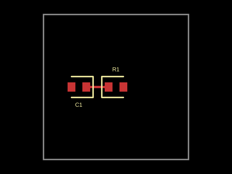 More from this authormohan-bee/repro-2This code defines a 10x10mm circuit board featuring a 1kΩ resistor and a 1000pF capacitor connected via 0402 footprint components.
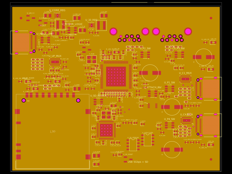 Similar packagegokul/usb3-sd-hubEngineering draft: four-layer, computer-powered USB 3 hub with one USB-C host socket, two USB-C and two USB-A accessory sockets, and a full-size SD slot. Board and three schematic previews are available. Routing and production checks are incomplete; not fabrication ready.
 Discover something newhrithik18k/punck-tscircuit-recreationA four-layer Eurorack drum/sampler controller PCB built around an STM32H743, dual QSPI flash, PCM5100 stereo DAC, TL074 analog audio circuitry, input clamps, 12V-to-3.3V power regulation, MIDI/USB/SWD connectors, controls, LEDs, and trigger/audio I/O.