README.md
# T113 Minimal Linux — Rev A

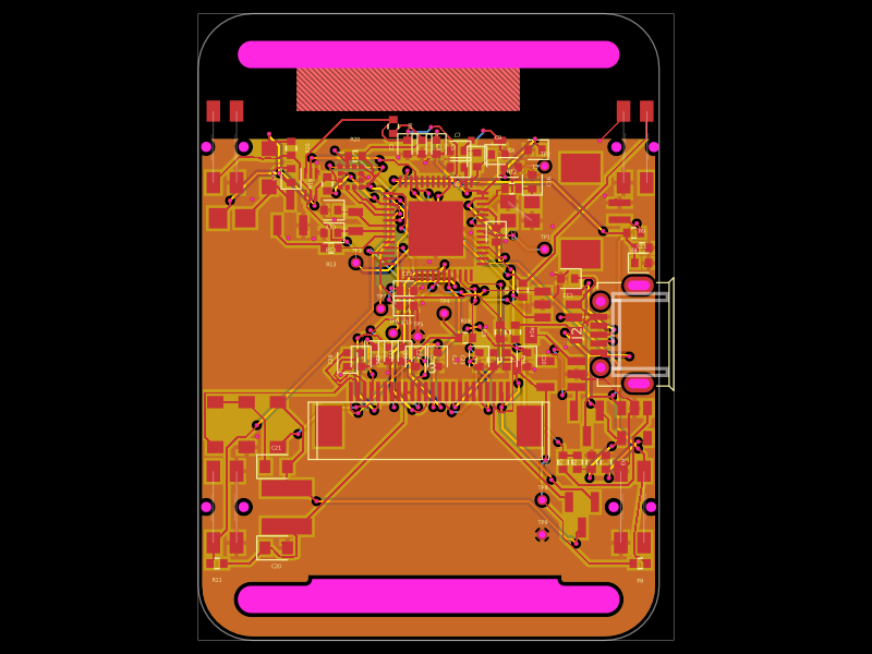
A four-layer Allwinner T113-S3 engineering prototype with integrated 128 MB DDR3, microSD boot storage, USB-C device/recovery, a 3.3 V UART header, and sequenced power supplies. The PCB is 140 × 120 mm to keep the first revision accessible for measurement and bring-up.

This is a design prototype. Hardware boot, signal integrity, power transients, and assembly have not been tested on a manufactured board. A board-specific bootloader and Linux device tree are required.

## Design

- T113-S3 eLQFP128 and exposed ground pad; 24 MHz and 32.768 kHz resonators and local decoupling.
- 1.8 V RTC supply, then 3.3 V I/O, followed by 0.9 V core and 1.5 V DDR. Supervisor delays hold reset while the supplies settle. LDOB is not connected to DDR power.
- One USB-C input with two separate 5.1 kΩ CC resistors, a 1.1 A resettable fuse, USBLC6 ESD protection, and an isolated, active-low VBUS indication on PD22. No USB-PD controller is fitted.
- MicroSD socket with pull-ups and a 33 Ω source-series clock resistor.
- Three-pin UART header: 1 GND, 2 TX, 3 RX, from the T113 viewpoint; 1 kΩ series resistors. Use a 3.3 V USB-UART adapter.
- Reset, PC4 boot-select control, and rail probe points. Test points are bare PCB features and are excluded from assembly.

The processor schematic shows the used pins. The complete 129-pin footprint and explicit NC declarations for unused pins remain in the source and Circuit JSON.

## Layout and checks

Schematic placement uses Matchpack; schematic connections use `SchematicTracePipelineSolver`. The UART connector group uses `pcbPack`; critical SoC, clock, power, and USB placements are fixed. Schematic sheets use A4. Formal Circuit JSON warning/error counts are recorded separately from runtime solver iteration diagnostics.

The independent checks in `scripts/check-design.py` verify supply and interface pin numbers, the reset/enable chain, regulator divider values, unused-pin declarations, and physical SoC pin coverage. `scripts/check-routing.py` checks actual copper connectivity, clearances, drill spacing, and board-edge clearance with Shapely.

See `routing/validation.json` for the final results and exact file hashes. The source build log retains IRLS iteration-limit diagnostics, and the Gerber check retains its parser’s unsupported paste-rotation diagnostics; zero formal schematic warnings does not mean every external tool emits no diagnostics. Source edits require rebuilding and rerouting; saved routes must not be attached to a changed placement or netlist.

## Manufacturing and bring-up

- Review the fabricator's four-layer stackup and calculate the USB differential impedance for its actual materials. The intended outer USB geometry is 0.15 mm tracks with a 0.16 mm edge gap; this alone does not certify 90 Ω impedance.
- Thermal vias inside the SoC exposed pad and the documented via-in-pad locations require resin filling, planarization, and copper caps. Ordinary open vias or soldermask tenting are not substitutes for this assembly process.
- Use a current-limited 5 V source for initial power checks. Confirm every rail and reset timing before fitting boot media or expecting the SoC to boot.
- The PC4 switch is a boot-select control, not a verified forced-FEL button. With no bootable media installed, reset and check USB0 ROM recovery and the UART console.
- Select and review the exact passive BOM parts, voltage ratings, crystal loading, USB assembly, and exposed-pad stencil before ordering assembled boards.

## Local commands

```sh
bun install --frozen-lockfile
bun run typecheck
bun run build:source
python -m venv .venv
.venv/bin/pip install -r requirements-routing.txt
.venv/bin/python scripts/check-design.py dist/index/circuit.json
.venv/bin/python scripts/check-schematic.py dist/index/circuit.json dist/solver-debug/index/solver-inputs.json
.venv/bin/python scripts/check-routing.py routed.circuit.json
bun scripts/render-previews.mjs routed.circuit.json
```

Fresh PCB routing retains checked reference copper and uses the remaining-net grid router with exact copper obstacles and validated through-via sites. The routing procedure and checks are recorded in `ROUTING.md`.

## References and attribution

The source is derived from [Seve's T113 Workbench, version 0.1.0](https://tscircuit.com/seveibar/allwinner-t113-dev-board), with the expansion headers, display/audio facilities, and USB-UART bridge removed. Its imported component definitions, sequenced-power design, protected power/USB geometry, and geometric routing tools were adapted for this board. The original registry package has no stated license; this project does not assign a new license to that upstream material.

Electrical reference: [Allwinner T113-S3 datasheet v1.6](https://dl.100ask.net/Hardware/MPU/100ask_t113-pro/T113-s3_datasheet_v1.6.pdf), including the pin tables, supply specifications, and §5.12 sequencing requirements. Also consulted: the [MangoPi MQ-Dual v1.6 schematic](https://widora.cn/_media/mq-dual_sch_v1.6.pdf).