krishnax12/t113-minimal-linux
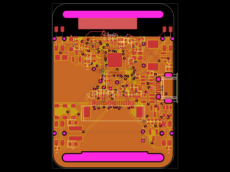
Allwinner T113-S3 dual-Cortex-A7 SoC with integrated 128MB DDR3, multi-rail decoupling, 24MHz and 32.768kHz oscillators, filtering, and exposed test points.
- Version
- 0.1.1
- License
- unset
- Stars
- 0
index.circuit.tsx
PCB

Schematic

import { Fragment } from "react"
import { Core } from "./circuits/Core"
import Power, { Buck } from "./circuits/Power"
import { StorageDebug } from "./circuits/StorageDebug"
import { UsbSense } from "./circuits/UsbSense"
import { Usb } from "./circuits/Usb"
import { Silk, TP } from "./circuits/helpers"

export default function T113MinimalLinux() {
  return (
    <board
      title="T113 Minimal Linux Rev A"
      width={140}
      height={120}
      borderRadius={3}
      layers={4}
      thickness={1.6}
      isViaInPadAllowed
      solderMaskColor="blue"
      silkscreenColor="white"
      routingDisabled
      schMatchAdapt
      schTraceAutoLabelEnabled
      schMaxTraceDistance={4}
      pcbStyle={{
        silkscreenFontSize: 0.65,
        viaHoleDiameter: 0.3,
        viaPadDiameter: 0.6,
      }}
      minTraceWidth={0.15}
    >
      <net name="GND" isGroundNet />
      <net name="V5" isPowerNet nominalTraceWidth={0.6} />
      <net name="V3V3" isPowerNet nominalTraceWidth={0.4} />
      <net name="V0V9" isPowerNet nominalTraceWidth={0.4} />
      <net name="V1V5" isPowerNet nominalTraceWidth={0.4} />
      <net name="VRTC1V8" isPowerNet nominalTraceWidth={0.2} />
      <net name="LDOA1V8" isPowerNet nominalTraceWidth={0.2} />
      <net name="LDOB_OUT" isPowerNet nominalTraceWidth={0.2} />
      <schematicsheet
        name="Processor"
        displayName="T113-S3 processor and clocks"
        sheetSize="A4"
      >
        <Core />
      </schematicsheet>
      <schematicsheet name="IO Supply" displayName="3.3 V I/O supply">
        <Buck
          id={101}
          py={4}
          upper="453k"
          out="V3V3"
          enable="EN_IO"
          link={107}
        />
      </schematicsheet>
      <schematicsheet name="Core Supply" displayName="0.9 V core supply">
        <Buck
          id={102}
          py={-12}
          upper="49.9k"
          out="V0V9"
          enable="EN_CORE_DDR"
          link={108}
        />
      </schematicsheet>
      <schematicsheet name="DDR Supply" displayName="1.5 V DDR supply">
        <Buck id={103} py={-28} upper="150k" out="V1V5" enable="EN_CORE_DDR" />
      </schematicsheet>
      <schematicsheet
        name="Power"
        displayName="Sequenced power supplies"
        sheetSize="A4"
      >
        <Power />
        {["V5", "VRTC1V8", "V3V3", "V0V9", "V1V5", "GND"].map((net, index) => (
          <TP
            key={net}
            name={`TP_RAIL${index}`}
            net={net}
            x={-59 + index * 6}
            y={-48}
          />
        ))}
      </schematicsheet>
      <schematicsheet
        name="Interfaces"
        displayName="USB, microSD and UART"
        sheetSize="A4"
      >
        <Usb />
        <UsbSense />
        <StorageDebug />
      </schematicsheet>
      {[
        [-65, -50],
        [-65, 50],
        [35, -50],
        [35, 50],
      ].map(([x, y], index) => (
        <Fragment key={index}>
          <hole name={`H${index + 1}`} diameter={3.2} pcbX={x} pcbY={y} />
        </Fragment>
      ))}
      <Silk text="T113 MINIMAL LINUX" x={-15} y={48} size={2} />
      <Silk text="REV A / 4 LAYERS / 128MB DDR3" x={-15} y={44.5} size={0.9} />
      <Silk text="KRISHNAX12 / PROTOTYPE" x={12} y={-46} size={0.9} />
    </board>
  )
}
Related Packages
 More from this authorkrishnax12/watchy-eink-smartwatchUnfinished prototype (not production-ready): 4 native DRC errors, 2 display-flex intersections, and missing antenna radiator copper remain
 Similar packageliammcg/BayFinder_V1_REVC_ESP32_CARRIERThis design implements a control PCB assembly featuring multiple headers (J1–J4) for ESP32-S3 module connection, integrated USB Type-B and A connectors (J5, J6) for power and data, a protected 5V power circuitry with fuses and TVS diode, an onboard SSD1306 OLED display (J8), and mechanical DIN-rail mounting holes, all interconnected with signal traces, ground pours, and test points.
 Discover something newShiboSoftwareDev/muse-aipi-lite-replacementA four-layer ESP32-S3 carrier board with USB‑C 5V input, AMS1117 3.3V regulation, FFC display/interface connector, status LED, reset/boot/user buttons, decoupling passives, test points, and ground/power planes.