shibosoftwaredev/f1c100s-linux-nema17-stepper-controller
A four-layer NEMA 17 motor-controller PCB combining an Allwinner F1C100S Linux computer, USB‑PD/buck power system, W5500 Ethernet, STM32 real-time motion control, DRV8825 stepper driver, protection/temperature/current telemetry, USB interfaces, and local LED/buzzer diagnostics.
- Version
- 0.4.56
- License
- unset
- Stars
- 0
usb-attach.tsx
const sheet={schSheetName:"usb_attach"} as const
const link=({name,from,to}:{name:string,from:string,to:string})=><trace name={name} from={from} to={to} thickness={.12} />

/** Hardware disconnect also applies to the F1C100S ROM FEL pull-up.
 * Host VBUS only supplies the NPN base through 47k; it never powers a board
 * rail. OE is pulled HIGH (disconnect) unless that VBUS drives Q_USB_ATTACH.
 * The 100k base pulldown prevents a floating base after cable removal.
 */
export function UsbAttach() {
  return <group name="USB_ATTACH" pcbX={0} pcbY={0} {...sheet}>
    <chip name="U_USB_GATE" manufacturerPartNumber="TS3USB31ERSER"
      supplierPartNumbers={{jlcpcb:["C967436"]}} layer="top"
      pcbX={-9.4} pcbY={11} schX={0} schY={2} schWidth={1.15} schHeight={1.5}
      pinLabels={{pin1:"N_OE",pin2:"HSD_P",pin3:"D_P",pin4:"GND",pin5:"D_N",pin6:"HSD_N",pin7:"NC",pin8:"VCC"}}
      pinAttributes={{pin1:{isInput:true},pin7:{doNotConnect:true},pin4:{requiresGround:true},pin8:{requiresPower:true,requiresVoltage:3.3}}}
      schPinArrangement={{leftSide:[3,5,1],rightSide:[2,6],topSide:[8],bottomSide:[4,7]}}
      footprint={<footprint>
        {/* TI RSE0008A, drawing 4220323/B, top-view land pattern. */}
        <smtpad portHints={["pin1"]} pcbX={-.675} pcbY={.5} width={.55} height={.25} shape="rect" />
        <smtpad portHints={["pin2"]} pcbX={-.675} pcbY={0} width={.55} height={.2} shape="rect" />
        <smtpad portHints={["pin3"]} pcbX={-.675} pcbY={-.5} width={.55} height={.25} shape="rect" />
        <smtpad portHints={["pin4"]} pcbX={0} pcbY={-.65} width={.3} height={.6} shape="rect" />
        <smtpad portHints={["pin5"]} pcbX={.675} pcbY={-.5} width={.55} height={.25} shape="rect" />
        <smtpad portHints={["pin6"]} pcbX={.675} pcbY={0} width={.55} height={.2} shape="rect" />
        <smtpad portHints={["pin7"]} pcbX={.675} pcbY={.5} width={.55} height={.25} shape="rect" />
        <smtpad portHints={["pin8"]} pcbX={0} pcbY={.65} width={.3} height={.6} shape="rect" />
        <courtyardrect width={2.1} height={2.1} />
      </footprint>} />
    <chip name="Q_USB_ATTACH" manufacturerPartNumber="MMBT3904(RANGE:100-300)"
      supplierPartNumbers={{jlcpcb:["C20526"]}} layer="bottom"
      pcbX={-.6} pcbY={16} schX={-4.5} schY={-3.5} schWidth={1.5} schHeight={2}
      pinLabels={{pin1:"B",pin2:"E",pin3:"C"}}
      pinAttributes={{pin1:{isInput:true},pin2:{requiresGround:true},pin3:{isOutput:true,canUseOpenCollector:true,isUsingOpenCollector:true}}}
      schPinArrangement={{leftSide:[1],topSide:[3],bottomSide:[2]}}
      footprint={<footprint>
        <smtpad portHints={["pin1"]} pcbX={1} pcbY={-.95} width={1} height={.65} shape="rect" />
        <smtpad portHints={["pin2"]} pcbX={1} pcbY={.95} width={1} height={.65} shape="rect" />
        <smtpad portHints={["pin3"]} pcbX={-1} pcbY={0} width={1} height={.65} shape="rect" />
        <courtyardrect width={3.5} height={3.5} />
      </footprint>} />
    <resistor name="R_USB_BASE" resistance="47k" footprint="0402" layer="bottom"
      supplierPartNumbers={{jlcpcb:["C25792"]}} pcbX={-6} pcbY={11} schX={-8} schY={-3.5} />
    <resistor name="R_USB_BASE_PD" resistance="100k" footprint="0402" layer="bottom"
      supplierPartNumbers={{jlcpcb:["C25741"]}} pcbX={-4} pcbY={11} schX={-6.5} schY={-6} schRotation={-90} />
    <resistor name="R_USB_OE_PU" resistance="10k" footprint="0402" layer="bottom"
      supplierPartNumbers={{jlcpcb:["C25744"]}} pcbX={-7.6} pcbY={11.8} pcbRotation={90}
      schX={-4.5} schY={.5} schRotation={90} />
    <capacitor name="C_USB_GATE" capacitance="100nF" maxVoltageRating={16} footprint="0402" layer="top"
      supplierPartNumbers={{jlcpcb:["C1525"]}} pcbX={-11.4} pcbY={9.2} pcbRotation={90}
      schX={4} schY={4} schRotation={-90} maxDecouplingTraceLength={5} />
    {link({name:"USB_DATA_VBUS_JOIN",from:".J_USB_DATA > .pin15",to:".J_USB_DATA > .pin16"})}
    {link({name:"USB_DATA_VBUS_SENSE",from:".J_USB_DATA > .pin16",to:".R_USB_BASE > .pin1"})}
    {link({name:"USB_DATA_BASE",from:".R_USB_BASE > .pin2",to:".Q_USB_ATTACH > .B"})}
    {link({name:"USB_BASE_PD",from:".R_USB_BASE_PD > .pin1",to:".Q_USB_ATTACH > .B"})}
    {link({name:"USB_BASE_PD_GND",from:".R_USB_BASE_PD > .pin2",to:"net.BOARD_GND"})}
    {link({name:"USB_ATTACH_EMITTER",from:".Q_USB_ATTACH > .E",to:"net.BOARD_GND"})}
    {link({name:"USB_ATTACH_OE",from:".Q_USB_ATTACH > .C",to:".U_USB_GATE > .N_OE"})}
    {link({name:"USB_OE_PULLUP",from:".R_USB_OE_PU > .pin1",to:".U_USB_GATE > .N_OE"})}
    {link({name:"USB_OE_PULLUP_3V3",from:".R_USB_OE_PU > .pin2",to:".SOC .VCC_TV > .pin1"})}
    {link({name:"USB_GATE_VCC",from:".U_USB_GATE > .VCC",to:".C_USB_GATE > .pin1"})}
    {link({name:"USB_GATE_SUPPLY",from:".U_USB_GATE > .VCC",to:".SOC .VCC_TV > .pin1"})}
    {link({name:"USB_GATE_GND",from:".U_USB_GATE > .GND",to:"net.BOARD_GND"})}
    {link({name:"USB_GATE_BYPASS_GND",from:".C_USB_GATE > .pin2",to:"net.BOARD_GND"})}
    {/* The two SPST channels are symmetric: use channel 2 for USB P and
        channel 1 for USB N on BOTH ends. No pair polarity is exchanged.
        This aligns VCC/GND and both SoC-side exits with the existing fanout. */}
    {link({name:"USB_GATE_HOST_P",from:".U_USB_ESD > .pin4",to:".U_USB_GATE > .D_N"})}
    {link({name:"USB_GATE_HOST_N",from:".U_USB_ESD > .pin6",to:".U_USB_GATE > .D_P"})}
    {link({name:"USB_GATE_SOC_P",from:".U_USB_GATE > .HSD_N",to:"net.USB_P"})}
    {link({name:"USB_GATE_SOC_N",from:".U_USB_GATE > .HSD_P",to:"net.USB_N"})}
  </group>
}
Related Packages
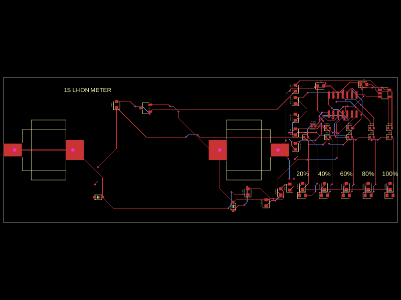 More from this authorShiboSoftwareDev/clip-on-battery-meter-2The code defines virtual representations of various electronic components—such as a BAT54WS Schottky diode and LM339 and LM393 voltage comparators—with physical pin configurations, footprints, and 3D models for PCB design.
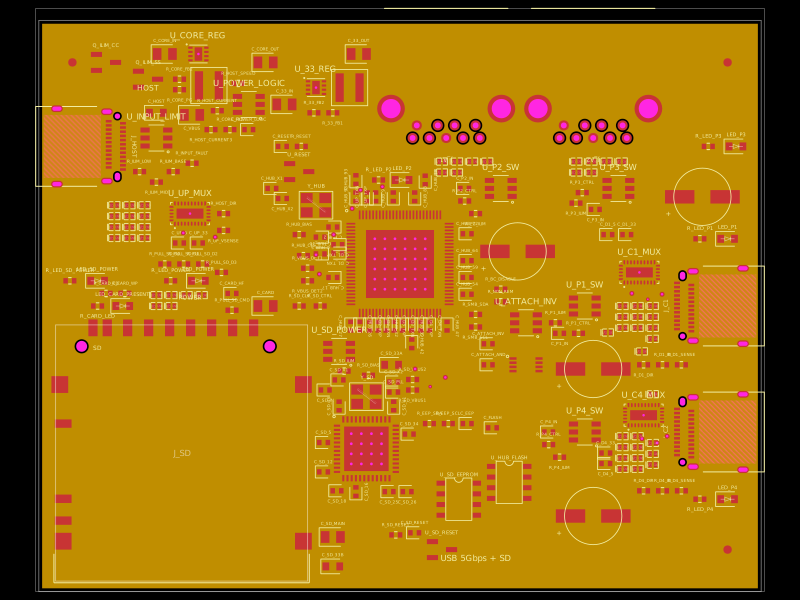 Similar packagegokul/usb3-sd-hubEngineering draft: four-layer, computer-powered USB 3 hub with one USB-C host socket, two USB-C and two USB-A accessory sockets, and a full-size SD slot. Board and three schematic previews are available. Routing and production checks are incomplete; not fabrication ready.
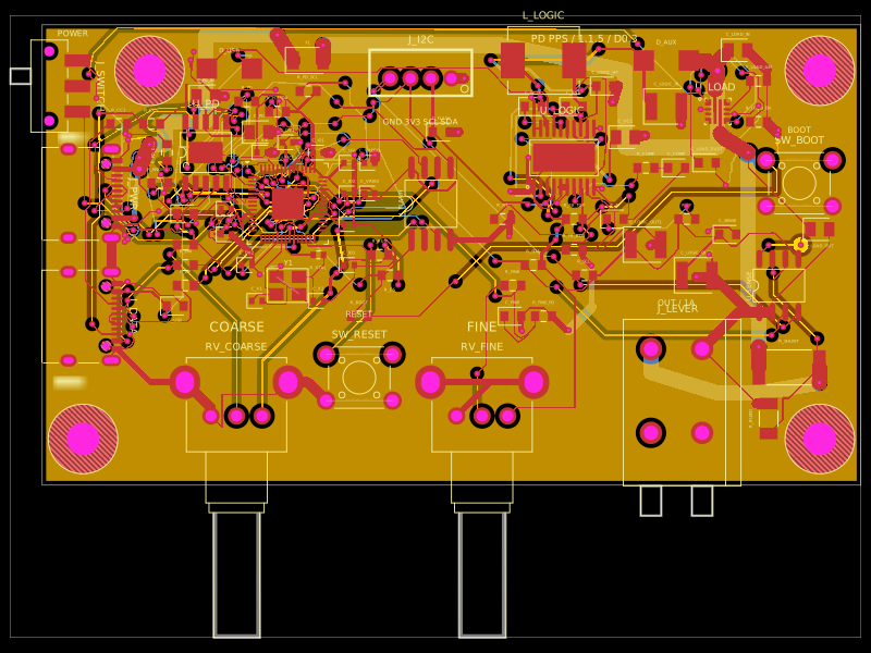 Discover something newastra/pd-power-supplyUSB-PD Power Supply with RP2040 controller