shibosoftwaredev/f1c100s-linux-nema17-stepper-controller
A four-layer NEMA 17 motor-controller PCB combining an Allwinner F1C100S Linux computer, USB‑PD/buck power system, W5500 Ethernet, STM32 real-time motion control, DRV8825 stepper driver, protection/temperature/current telemetry, USB interfaces, and local LED/buzzer diagnostics.
- Version
- 0.4.56
- License
- unset
- Stars
- 0
scripts/review-round2-geometry.py
"""Additional read-only coverage: mixed drills and populated signal via-in-pad.

Distances are geometry evidence, not an assertion of CAM acceptance. The
published JLC table does not separately define mixed via/PTH pair spacing.
"""
from route_geometry import *
from shapely.ops import unary_union
import hashlib
import sys

source = Path("dist/index/circuit.json")
c = load_circuit(str(source))
out = Path(sys.argv[1])
root = connectivity(c)
parts = {e["source_component_id"]: e for e in c if e["type"] == "source_component"}
placed = {e["pcb_component_id"]: e for e in c if e["type"] == "pcb_component"}
ports = {e["pcb_port_id"]: e for e in c if e["type"] == "pcb_port"}
source_ports = {e["source_port_id"]: e for e in c if e["type"] == "source_port"}
vias = [e for e in c if e["type"] == "pcb_via"]
pths = [e for e in c if e["type"] == "pcb_plated_hole"]
npths = [e for e in c if e["type"] == "pcb_hole"]
lands = [e for e in c if e["type"] == "pcb_smtpad"]

def part(e):
    return parts[placed[e["pcb_component_id"]]["source_component_id"]]

def drill(e):
    if e["type"] == "pcb_via":
        return Point(e["x"], e["y"]).buffer(e["hole_diameter"] / 2, quad_segs=32)
    return geometry(e, "hole_" if "hole_diameter" in e or "hole_width" in e else "")

mixed = []
for v in vias:
    for h in pths:
        distance = drill(v).distance(drill(h))
        if distance < .45:
            mixed.append(dict(via=v["pcb_via_id"], x=v["x"], y=v["y"],
                pth=h["pcb_plated_hole_id"], part=part(h)["name"], gapMm=round(distance, 6)))

via_in_populated_pad = []
for v in vias:
    hole = drill(v)
    for land in lands:
        component = part(land)
        if component.get("ftype") == "simple_test_point" or component.get("is_dnp"):
            continue
        if component.get("supplier_part_numbers", {}).get("jlcpcb") is None:
            continue
        area = hole.intersection(geometry(land)).area
        if area < 1e-7:
            continue
        p = source_ports.get(ports.get(land.get("pcb_port_id"), {}).get("source_port_id"), {})
        via_in_populated_pad.append(dict(via=v["pcb_via_id"], x=v["x"], y=v["y"],
            part=component["name"], pin=p.get("pin_number"), pinName=p.get("name"),
            layer=land["layer"], overlapAreaMm2=round(area, 6),
            fullDrillWithinLand=geometry(land).covers(hole),
            viaMaskFields={k: value for k, value in v.items() if "mask" in k or "tent" in k or "fill" in k}))

silk = [e for e in c if e["type"] == "pcb_silkscreen_text"]
outside_anchors = [dict(text=e["text"], layer=e["layer"], position=e["anchor_position"])
    for e in silk if max(abs(e["anchor_position"][a]) for a in ["x", "y"]) > 21.15]
jack = next(e for e in placed.values() if parts[e["source_component_id"]]["name"] == "J_ETH")
jack_envelope = box(jack["center"]["x"] - jack["width"]/2,
    jack["center"]["y"] - jack["height"]/2,
    jack["center"]["x"] + jack["width"]/2,
    jack["center"]["y"] + jack["height"]/2)
pour_overlap = {}
for layer in LAYERS:
    copper = []
    for e in c:
        if e["type"] != "pcb_copper_pour" or e["layer"] != layer:
            continue
        b = e["brep_shape"]
        ring = lambda r: [(v["x"], v["y"]) for v in r["vertices"]]
        copper.append(Polygon(ring(b["outer_ring"]), [ring(r) for r in b.get("inner_rings", [])]).buffer(0))
    pour_overlap[layer] = round(unary_union(copper).intersection(jack_envelope).area, 4)
report = dict(circuitSha256=hashlib.sha256(source.read_bytes()).hexdigest(),
    mixedDrillPairsBelowConservative045mm=len(mixed), mixedDrillPairs=mixed,
    mixedDrillCaveat="CAM confirmation needed: published via-via and PTH-PTH limits differ; mixed-pair rule not separately specified.",
    populatedPadDrillIntersections=via_in_populated_pad,
    viaInPadCaveat="Thermal pads may deliberately contain vias; signal-pad intersections need solder-process/filled-capped-via review. No fill process is inferred from the model.",
    minimumViaToNpthMm=min(drill(v).distance(drill(h)) for v in vias for h in npths),
    jackPcbEnvelopePourOverlapMm2=pour_overlap,
    jackPourCaveat="Intersects the emitted PCB component envelope, not an independently measured magnetics-core volume; all emitted pours are BOARD_GND. Review the actual jack exclusion region against the WIZnet guide.",
    silkscreenTexts=len(silk), smallTextCount=sum(e["font_size"] < 1 for e in silk),
    silkscreenAnchorsOutsideOutline=outside_anchors)
(out / "expanded-geometry.json").write_text(json.dumps(report, indent=2) + "\n")
print(json.dumps({k: v for k, v in report.items() if k not in ["mixedDrillPairs", "populatedPadDrillIntersections"]}))
print(json.dumps(via_in_populated_pad))
Related Packages
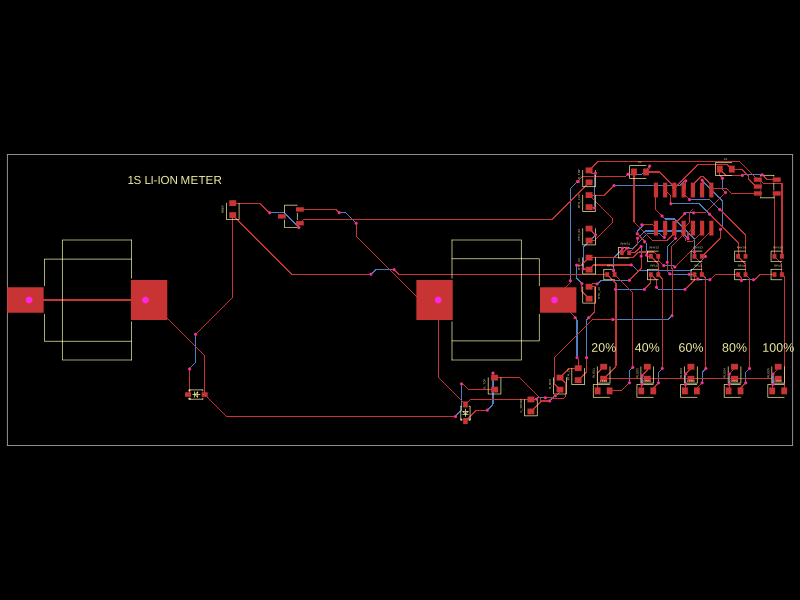 More from this authorShiboSoftwareDev/clip-on-battery-meter-2The code defines virtual representations of various electronic components—such as a BAT54WS Schottky diode and LM339 and LM393 voltage comparators—with physical pin configurations, footprints, and 3D models for PCB design.
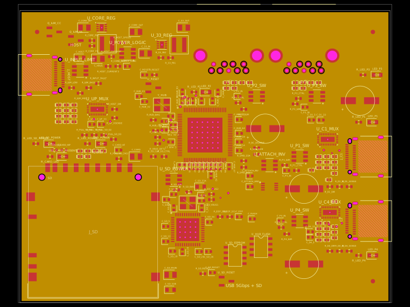 Similar packagegokul/usb3-sd-hubEngineering draft: four-layer, computer-powered USB 3 hub with one USB-C host socket, two USB-C and two USB-A accessory sockets, and a full-size SD slot. Board and three schematic previews are available. Routing and production checks are incomplete; not fabrication ready.
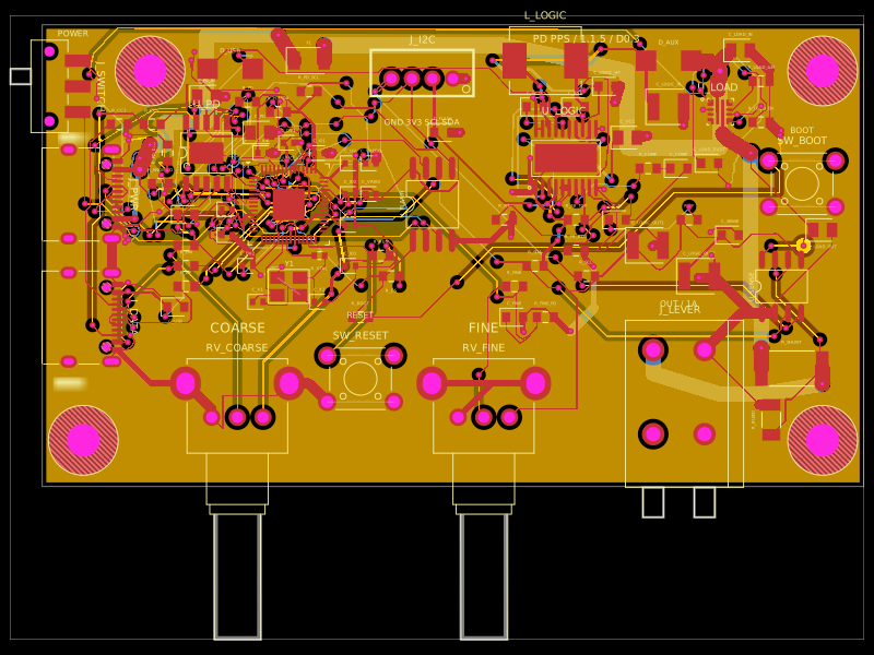 Discover something newastra/pd-power-supplyUSB-PD Power Supply with RP2040 controller