shibosoftwaredev/f1c100s-linux-nema17-stepper-controller
A four-layer NEMA 17 motor-controller PCB combining an Allwinner F1C100S Linux computer, USB‑PD/buck power system, W5500 Ethernet, STM32 real-time motion control, DRV8825 stepper driver, protection/temperature/current telemetry, USB interfaces, and local LED/buzzer diagnostics.
- Version
- 0.4.56
- License
- unset
- Stars
- 0
scripts/export-whole-board.py
"""Export a new four-layer job containing pads and mechanical obstacles only.
No copper from the previous design is loaded into this routing job.
"""
from route_geometry import *
from collections import defaultdict
import os

circuit = load_circuit("routing/placement.json" if os.environ.get("READ_PLACEMENT") else "dist/index/circuit.json")
root = connectivity(circuit)
ports = {e["pcb_port_id"]: e for e in circuit if e["type"] == "pcb_port"}
source_traces = {e["source_trace_id"]: e for e in circuit if e["type"] == "source_trace"}
source_ports = {e["source_port_id"]: e for e in circuit if e["type"] == "source_port"}
sources = {e["source_component_id"]: e for e in circuit if e["type"] == "source_component"}
u = lambda x: f"{x * 1000:.4f}"
xy = lambda x, y: u(x) + " " + u(y)
def polygon(g, layer):
    return f"(polygon {layer} 0 " + " ".join(xy(x, y) for x, y in list(g.exterior.coords)[:-1]) + ")"

net_names = defaultdict(list)
for e in circuit:
    if e["type"] == "source_net":
        net_names[root(e["source_net_id"])].append(e["name"])
net_ids = {}
def net_for(e):
    pid = e.get("pcb_port_id")
    key = root(ports[pid]["source_port_id"]) if pid in ports else "NC_" + e[e["type"] + "_id"]
    if key not in net_ids:
        net_ids[key] = f"N{len(net_ids)}"
    return net_ids[key]

images, stacks, places, keepouts = [], [], [], []
pins, pinmap = defaultdict(list), {}
for e in circuit:
    typ = e["type"]
    if typ in ["pcb_smtpad", "pcb_plated_hole"]:
        net = net_for(e)
        g = geometry(e, "outer_" if typ == "pcb_plated_hole" else "")
        # Polygon pads express their vertices in board coordinates.
        x, y = (e["x"], e["y"]) if "x" in e else (g.centroid.x, g.centroid.y)
        layers = e.get("layers", [e.get("layer")])
        name, stack = f"P{len(images)}", f"S{len(stacks)}"
        local = translate(g, -x, -y)
        stacks.append(f"(padstack {stack} " + " ".join(
            "(shape " + polygon(local, layer) + ")" for layer in layers) + " (attach off))")
        images.append(f"(image {name} (pin {stack} 1 0 0))")
        places.append(f"(component {name} (place {name} {xy(x,y)} front 0))")
        pins[net].append(name + "-1")
        pinmap[name] = {"element": e[typ+"_id"], "pcb_port_id": e.get("pcb_port_id"), "net": net}
        if typ == "pcb_plated_hole":
            drill = geometry(e, "hole_").buffer(.275)
            keepouts.extend(f"(via_keepout V{len(keepouts)+i} {polygon(drill,l)})"
                            for i,l in enumerate(LAYERS))
    elif typ == "pcb_hole":
        g = geometry(e, "hole_" if "hole_diameter" in e else "").buffer(.2)
        keepouts.extend(f"(keepout H{len(keepouts)+i} {polygon(g,l)})" for i,l in enumerate(LAYERS))

# Keep exposed traces and vias clear of the normal M3 socket heads and rear
# standoffs. The motor outline and mounting-hole centers are unchanged.
for x in [-15.5, 15.5]:
    for y in [-15.5, 15.5]:
        for layer, radius in [("top", 2.85), ("bottom", 2.6)]:
            g = Point(x,y).buffer(radius, quad_segs=16)
            keepouts.append(f"(keepout SCREW{len(keepouts)} {polygon(g,layer)})")

# Wide load paths and switch nodes stay on outer copper. Fine-pitch signal
# and low-current rail branches use all four layers with 0.12 mm traces.
wide = {}
outer_ids = {"source_trace_83", "source_trace_84", "source_trace_110",
             "source_trace_303", "source_trace_304", "source_trace_381"}
top_only = set()
for t in source_traces.values():
    ids = t.get("connected_source_port_ids", []) + t.get("connected_source_net_ids", [])
    if not ids:
        continue
    key = root(ids[0])
    net = net_ids.get(key)
    if not net:
        continue
    name = t.get("name", "")
    if t["source_trace_id"] in outer_ids or name in ["VM_PROTECTED", "DRV_VMA", "DRV_VMB"]:
        wide[net] = max(wide.get(net, 0), .5)
    if name in ["USB_VBUS_A", "USB_VBUS_B", "BUCK_SW", "BUCK_OUT"]:
        wide[net] = max(wide.get(net, 0), .8)
    if name.startswith(("VBUS_SOURCE_", "VBUS_DRAIN_")):
        wide[net] = max(wide.get(net, 0), .6)
    if name.startswith("MOTOR_") and name.endswith(("PLUS", "MINUS")):
        wide[net] = max(wide.get(net, 0), .3)
    if name in ["BUCK_SW", "BUCK_OUT", "BUCK_OUT1", "BUCK_OUT2"]:
        wide[net] = max(wide.get(net, 0), .4)
    if name in ["N_HOSCI", "N_HOSCO", "ETH_XI", "ETH_XO", "ETH_XI_CAP", "ETH_XO_CAP"]:
        top_only.add(net)

classes = []
width_floors=json.loads(Path('routing/required-net-widths.json').read_text()) if Path('routing/required-net-widths.json').exists() else {}
for net in pins:
    # The wide load paths are explicitly routed/protected in final-job.dsn.
    # Do not impose their width/layer rule on weak pull-ups and divider taps
    # sharing the same electrical rail. Those branches retain their own
    # source minimums; the emitted load trunks are verified independently.
    branch_widths=[t.get("min_trace_thickness",.12) for t in source_traces.values()
                   if (t.get("connected_source_port_ids",[])+t.get("connected_source_net_ids",[]))
                   and net_ids.get(root((t.get("connected_source_port_ids",[])+t.get("connected_source_net_ids",[]))[0]))==net]
    width=max(min(branch_widths or [.12]),width_floors.get(net,0))
    layer_rule = " (use_layer top bottom)" if net in wide and (width>=wide[net] or net in width_floors) else ""
    # Ethernet oscillator is on the bottom, SoC crystal is on the top.
    if net in top_only:
        net_ports = [e for e in circuit if e["type"] == "pcb_smtpad" and net_for(e) == net]
        common = set(LAYERS)
        for e in net_ports:
            common &= {e["layer"]}
        if len(common) == 1:
            layer_rule = " (use_layer " + next(iter(common)) + ")"
    classes.append(f"(class C{len(classes)} {net} (circuit (use_via VIA){layer_rule}) "
                   f"(rule (width {u(width)}) (clearance 110)))")

board = next(e for e in circuit if e["type"] == "pcb_board")
boundary = Polygon([(p["x"],p["y"]) for p in board["outline"]]).buffer(-.30, join_style=2)
stacks.append("(padstack VIA " + " ".join(f"(shape (circle {l} 450))" for l in LAYERS) + " (attach off))")
text = '(pcb nema17\n(parser (string_quote ") (space_in_quoted_tokens on) (host_cad tscircuit))\n'
text += '(resolution um 10) (unit um)\n(structure\n'
text += "\n".join(f"(layer {l} (type signal) (property (index {i})))" for i,l in enumerate(LAYERS))
text += "\n(boundary (path pcb 0 " + " ".join(xy(x,y) for x,y in boundary.exterior.coords) + "))\n"
text += "\n".join(keepouts)
text += "\n(via VIA) (rule (width 120) (clearance 110) (clearance 125 (type via_smd)) (clearance 160 (type via_via))))\n"
text += "(placement " + "\n".join(places) + ")\n(library " + "\n".join(images+stacks) + ")\n"
text += "(network " + "\n".join(f"(net {n} (pins {' '.join(p)}))" for n,p in pins.items()) + "\n" + "\n".join(classes) + ")\n(wiring)\n)\n"
Path("routing/board.dsn").write_text(text)
Path("routing/placement.json").write_text(json.dumps(circuit, indent=2))
Path("routing/net-map.json").write_text(json.dumps({
    "roots": net_ids, "names": dict(net_names), "pinmap": pinmap,
    "outer": wide, "pin_counts": {k: len(v) for k,v in pins.items()},
}, indent=2))
driver=next(e for e in circuit if e["type"]=="pcb_component" and sources[e["source_component_id"]]["name"]=="U_MOTOR")
ground=next(t for t in source_traces.values() if t.get("name")=="DRV_EP_GND")
ground_net=net_ids[root(ground["connected_source_port_ids"][0])]
thermal=[{"x":round(driver["center"]["x"]+x,6),"y":round(driver["center"]["y"]+y,6),
          "net":ground_net,"source_trace_id":ground["source_trace_id"]}
         for y in [-1.2,-.4,.4,1.2] for x in [1.4,1.95,2.5] if (x,y)!=(2.5,1.2)]
pd=next(e for e in circuit if e["type"]=="pcb_component" and sources[e["source_component_id"]]["name"]=="U_PD")
pd_ground=next(t for t in source_traces.values() if t.get("name")=="PD_GROUND")
# Preserve the approved ground drill, not the 15 micrometre body/courtyard
# adjustment of U_PD. Both points are well inside the same exposed land.
auxiliary=[{"id":"pd_ground_0","x":round(pd["center"]["x"]+.015,6),"y":pd["center"]["y"],
            "net":ground_net,"source_trace_id":pd_ground["source_trace_id"]}]
Path("routing/native-features.json").write_text(json.dumps({"thermal_vias":thermal,"auxiliary_vias":auxiliary},indent=2)+"\n")
print(json.dumps({"pads": len(images), "nets": len(pins), "connected_nets": sum(len(p)>1 for p in pins.values()),
                  "keepouts": len(keepouts), "old_copper_objects": 0, "outer_load_nets": len(wide)}))
Related Packages
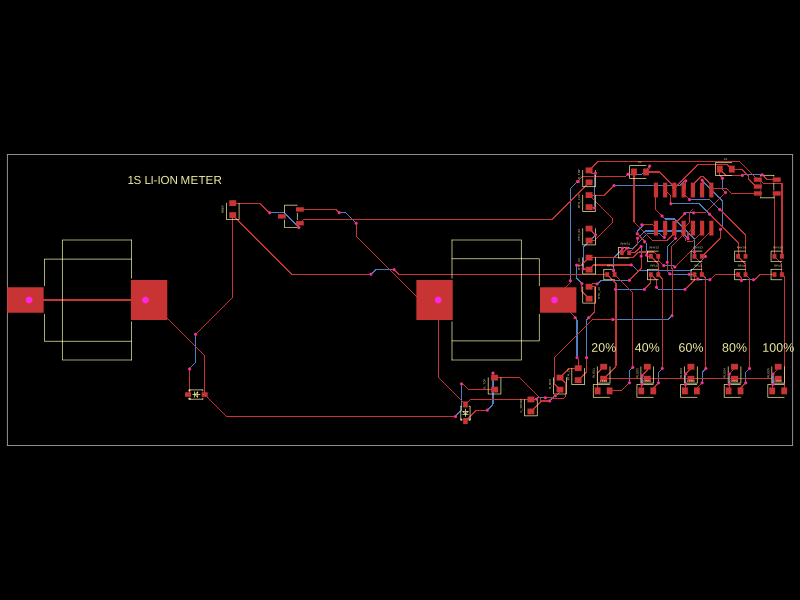 More from this authorShiboSoftwareDev/clip-on-battery-meter-2The code defines virtual representations of various electronic components—such as a BAT54WS Schottky diode and LM339 and LM393 voltage comparators—with physical pin configurations, footprints, and 3D models for PCB design.
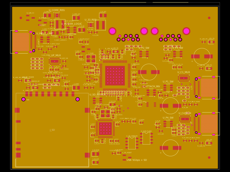 Similar packagegokul/usb3-sd-hubEngineering draft: four-layer, computer-powered USB 3 hub with one USB-C host socket, two USB-C and two USB-A accessory sockets, and a full-size SD slot. Board and three schematic previews are available. Routing and production checks are incomplete; not fabrication ready.
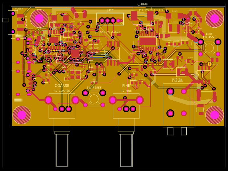 Discover something newastra/pd-power-supplyUSB-PD Power Supply with RP2040 controller