shibosoftwaredev/f1c100s-linux-nema17-stepper-controller
A four-layer NEMA 17 motor-controller PCB combining an Allwinner F1C100S Linux computer, USB‑PD/buck power system, W5500 Ethernet, STM32 real-time motion control, DRV8825 stepper driver, protection/temperature/current telemetry, USB interfaces, and local LED/buzzer diagnostics.
- Version
- 0.4.56
- License
- unset
- Stars
- 0
scripts/audit-solder-process.py
"""Hash-bound solder-process audit; tenting is not filled/capped via-in-pad."""
from route_geometry import *
import hashlib

path=Path("dist/index/circuit.json");c=load_circuit(str(path))
spec_path=Path("manufacturing-process.json")
spec=json.loads(spec_path.read_text()) if spec_path.exists() else {}
via_spec=spec.get("throughVias",{})
sources={e["source_component_id"]:e for e in c if e["type"]=="source_component"}
parts={e["pcb_component_id"]:e for e in c if e["type"]=="pcb_component"}
ports={e["pcb_port_id"]:e for e in c if e["type"]=="pcb_port"}
sp={e["source_port_id"]:e for e in c if e["type"]=="source_port"}
vias=[e for e in c if e["type"]=="pcb_via"]
ordinary=[];thermal=[]
for e in c:
    if e["type"]!="pcb_smtpad":continue
    pcb=parts[e["pcb_component_id"]];s=sources[pcb["source_component_id"]]
    if pcb.get("do_not_place") or s.get("ftype")=="simple_test_point":continue
    port=sp.get(ports.get(e.get("pcb_port_id"),{}).get("source_port_id"),{})
    for v in vias:
        area=Point(v["x"],v["y"]).buffer(v["hole_diameter"]/2,quad_segs=32).intersection(geometry(e)).area
        if area<1e-7:continue
        finding=dict(part=s["name"],pin=port.get("pin_number"),layer=e["layer"],via=v["pcb_via_id"],x=v["x"],y=v["y"],overlapAreaMm2=round(area,6))
        (thermal if (s["name"],port.get("pin_number")) in {("U1",89),("U_MOTOR",29),("U_PD",17)} else ordinary).append(finding)
specified=(via_spec.get("treatment")=="epoxy-filled-and-copper-capped" and
    via_spec.get("ipc4761Type")=="VII" and via_spec.get("finishedDrillMm")==.3 and
    via_spec.get("padDiameterMm")==.45 and via_spec.get("paidFourLayerOptionRequired") is True and
    set(via_spec.get("span",[]))==set(LAYERS) and via_spec.get("planarizedForSmtOnBothFaces") is True and
    bool(vias) and all(v["hole_diameter"]==.3 and v["outer_diameter"]==.45 and set(v["layers"])==set(LAYERS) for v in vias))
report=dict(circuitSha256=hashlib.sha256(path.read_bytes()).hexdigest(),approvedForAssembly=False,
    ordinaryPadDrillIntersections=ordinary,thermalPadDrillIntersections=thermal,
    specifiedFilledCappedProcess=specified,thermalStencilProcessQualified=False,
    processSpecificationSha256=hashlib.sha256(spec_path.read_bytes()).hexdigest() if spec_path.exists() else None,
    processSpecification="manufacturing-process.json" if spec_path.exists() else None,
    assemblerApprovalRecord=spec.get("approvalRecord"),
    caveat="Filled/capped processing is specified locally, not accepted by a fabricator. Ordinary intersections include partial grazes, not proven solder failures. Exposed thermal pads still need package-specific stencil and double-sided reflow qualification. Tenting is not filling/capping; assembly approval remains false.",
    ruleSource="https://jlcpcb.com/help/article/pcb-via-covering")
Path("reports/solder-process-audit.json").write_text(json.dumps(report,indent=2)+"\n")
print(json.dumps({k:v for k,v in report.items() if k not in ["ordinaryPadDrillIntersections","thermalPadDrillIntersections"]}|{"ordinaryIntersections":len(ordinary),"thermalIntersections":len(thermal)}))
Related Packages
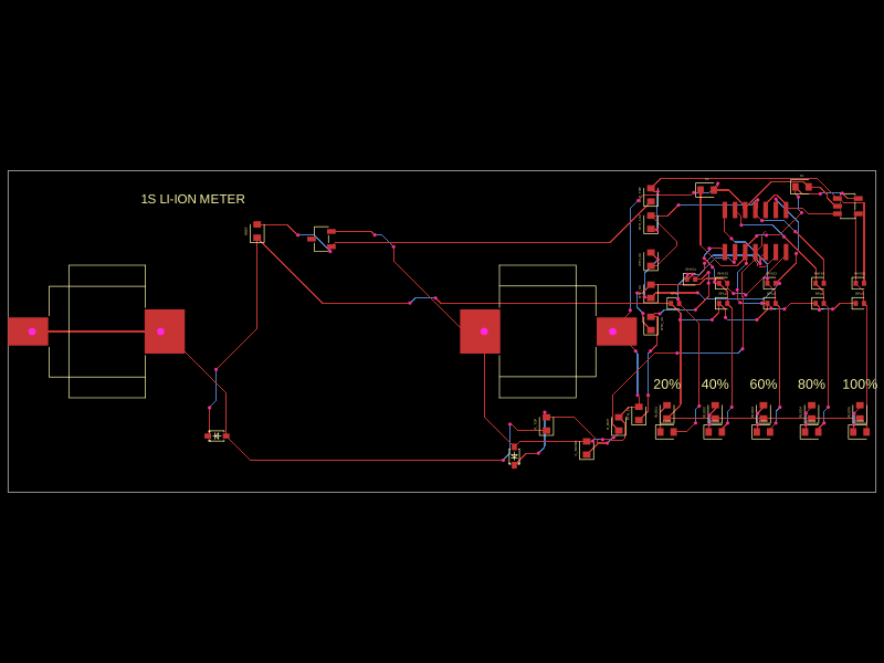 More from this authorShiboSoftwareDev/clip-on-battery-meter-2The code defines virtual representations of various electronic components—such as a BAT54WS Schottky diode and LM339 and LM393 voltage comparators—with physical pin configurations, footprints, and 3D models for PCB design.
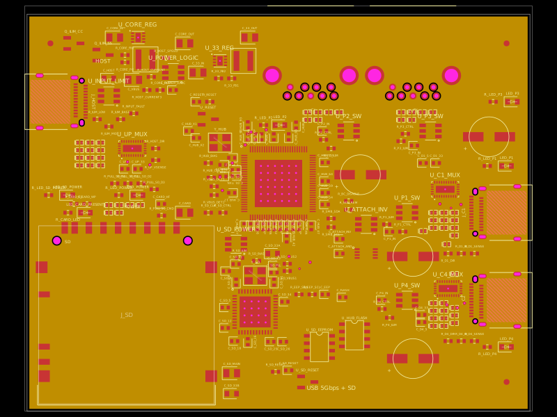 Similar packagegokul/usb3-sd-hubEngineering draft: four-layer, computer-powered USB 3 hub with one USB-C host socket, two USB-C and two USB-A accessory sockets, and a full-size SD slot. Board and three schematic previews are available. Routing and production checks are incomplete; not fabrication ready.
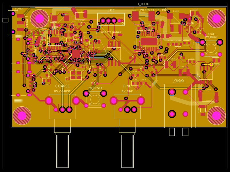 Discover something newastra/pd-power-supplyUSB-PD Power Supply with RP2040 controller