shibosoftwaredev/f1c100s-linux-nema17-stepper-controller
A four-layer NEMA 17 motor-controller PCB combining an Allwinner F1C100S Linux computer, USB‑PD/buck power system, W5500 Ethernet, STM32 real-time motion control, DRV8825 stepper driver, protection/temperature/current telemetry, USB interfaces, and local LED/buzzer diagnostics.
- Version
- 0.4.56
- License
- unset
- Stars
- 0
manufacturing-process.json
{
  "status": "specified-requires-fabricator-and-assembler-CAM-acceptance",
  "releaseApproved": false,
  "board": {
    "layers": 4,
    "thicknessMm": 1.6,
    "outlineMm": [42.3, 42.3],
    "surfaceFinish": "ENIG",
    "outerCopperOz": 1,
    "innerCopperOz": 0.5,
    "controlledImpedanceStackupQualified": false
  },
  "throughVias": {
    "finishedDrillMm": 0.3,
    "padDiameterMm": 0.45,
    "span": ["top", "inner1", "inner2", "bottom"],
    "treatment": "epoxy-filled-and-copper-capped",
    "ipc4761Type": "VII",
    "scope": "all pcb_via records; not connector plated holes or non-plated holes",
    "planarizedForSmtOnBothFaces": true,
    "paidFourLayerOptionRequired": true,
    "orderRemark": "4 layers, 1.6 mm, ENIG, 1 oz outer copper. Fill ALL 0.30 mm through vias with nonconductive epoxy resin and copper-cap/planarize both faces (IPC-4761 Type VII); 0.45 mm via lands. These include exposed thermal-pad vias. Tenting or solder-mask plugging is NOT an acceptable substitute. Do not fill component plated holes or non-plated mounting/locating holes. Confirm capability, price and finished-hole interpretation before manufacture.",
    "ruleSource": "https://jlcpcb.com/help/article/pcb-via-covering"
  },
  "assembly": {
    "faces": ["top", "bottom"],
    "throughHolePartsAreNotPinInPaste": true,
    "requirePasteOnEveryPopulatedExposedSmtLand": true,
    "stencilThicknessMm": null,
    "stencilAndReflowQualified": false,
    "request": "Review both paste layers and package-specific exposed-pad apertures. Select foil/step-stencil thickness for the fine-pitch F1C100S and PowerPAD driver, and agree thermal-pad paste volume, venting/voiding criteria, double-sided reflow order, bottom-component retention and through-hole soldering. Existing 0.7-linear signal-land reduction and thermal-pad apertures are proposed artwork, not approved process parameters.",
    "thermalPadReview": [
      {"part": "U1", "pin": 89, "package": "F1C100S exposed pad"},
      {"part": "U_MOTOR", "pin": 29, "package": "DRV8825 PowerPAD"},
      {"part": "U_PD", "pin": 17, "package": "HUSB238A exposed pad"}
    ],
    "ruleSource": "https://jlcpcb.com/help/article/instructions-for-stencil-order"
  },
  "approvalRecord": null,
  "caveat": "A locally specified process and supplied paste artwork are not evidence of accepted CAM, a placed order or qualified physical hardware. No cost is committed and no fabrication-ready flag may be inferred from this file."
}
Related Packages
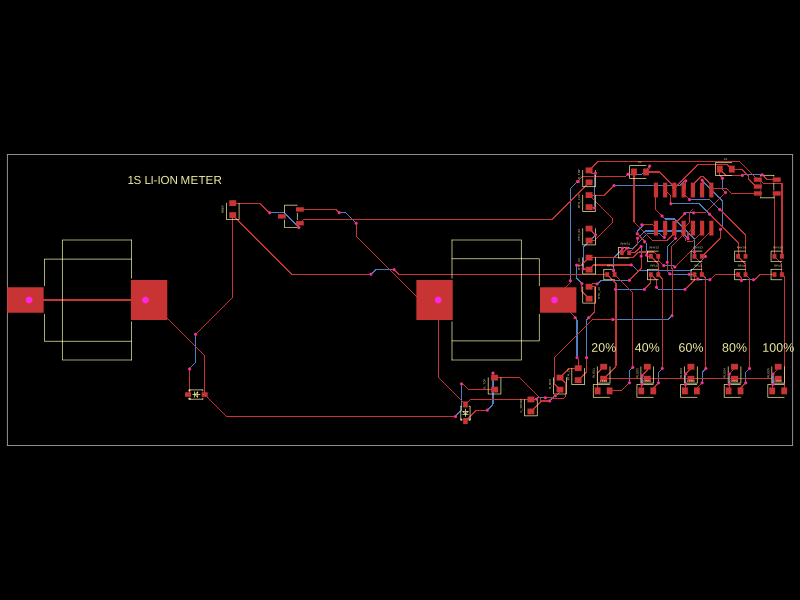 More from this authorShiboSoftwareDev/clip-on-battery-meter-2The code defines virtual representations of various electronic components—such as a BAT54WS Schottky diode and LM339 and LM393 voltage comparators—with physical pin configurations, footprints, and 3D models for PCB design.
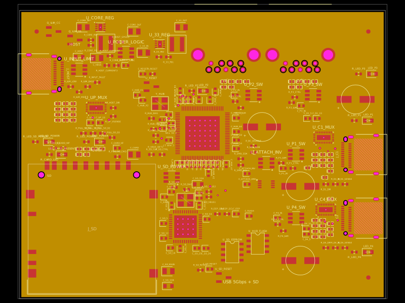 Similar packagegokul/usb3-sd-hubEngineering draft: four-layer, computer-powered USB 3 hub with one USB-C host socket, two USB-C and two USB-A accessory sockets, and a full-size SD slot. Board and three schematic previews are available. Routing and production checks are incomplete; not fabrication ready.
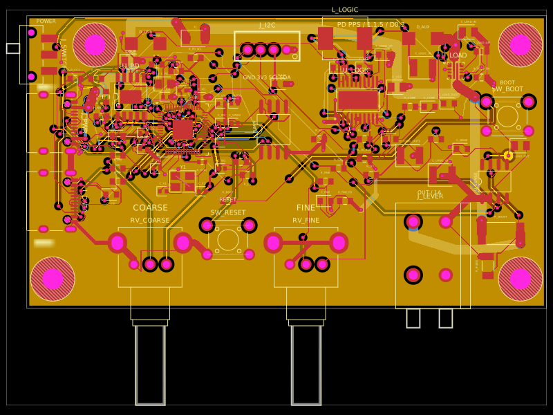 Discover something newastra/pd-power-supplyUSB-PD Power Supply with RP2040 controller