seveibar/minimal-rp2040
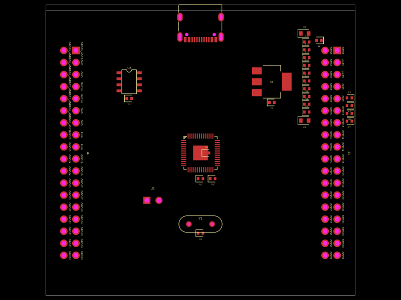
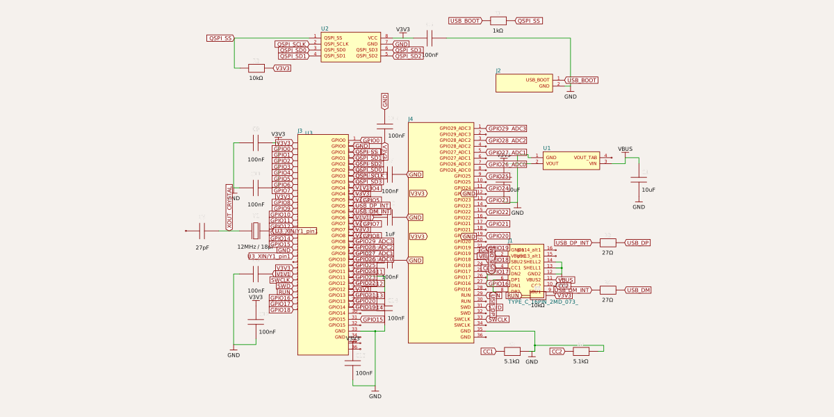
This design features a Raspberry Pi RP2040 microcontroller with integrated decoupling capacitors, QSPI flash memory, crystal oscillator, and USB power circuitry, all mounted on a 65mm by 60mm four-layer PCB.
Usage: To import and use the RP2040 component in a tscircuit project: 1. Import the component: ```tsx import { RP2040 } from "@tsci/seveibar.minimal-rp2040" ``` 2. Use the component in a board: ```tsx <board> <RP2040 name="U3" pcbX={0} pcbY={0} connections={{ IOVDD1: "net.V3V3", // Add other required connections }} /> </board> ``` Key points: - Specify a name for the component - Set position using `pcbX` and `pcbY` - Define necessary network connections in the `connections` prop - Ensure proper power and ground connections
- Version
- 1.0.1
- License
- unset
- Stars
- 1
USB_Micro-B_Amphenol_10103594-0001LF_Horizontal_modified.kicad_mod
PCB
Schematic
(module USB_Micro-B_Amphenol_10103594-0001LF_Horizontal_modified (layer F.Cu) (tedit 5F0317C2)
  (descr "Micro USB Type B 10103594-0001LF, http://cdn.amphenol-icc.com/media/wysiwyg/files/drawing/10103594.pdf")
  (tags "USB USB_B USB_micro USB_OTG")
  (attr smd)
  (fp_text reference J5 (at -5.365 -2.58 -180) (layer F.SilkS)
    (effects (font (size 1 1) (thickness 0.15)))
  )
  (fp_text value USB_B_Micro (at -0.025 3.32 -180) (layer F.Fab)
    (effects (font (size 1 1) (thickness 0.15)))
  )
  (fp_line (start 4.14 1.7) (end -4.13 1.7) (layer F.CrtYd) (width 0.05))
  (fp_line (start 4.14 1.7) (end 4.14 -3.995) (layer F.CrtYd) (width 0.05))
  (fp_line (start -4.13 -3.995) (end -4.13 1.7) (layer F.CrtYd) (width 0.05))
  (fp_line (start -4.13 -3.995) (end 4.14 -3.995) (layer F.CrtYd) (width 0.05))
  (fp_line (start -4.02 1.7) (end 4.02 1.7) (layer Dwgs.User) (width 0.1))
  (fp_line (start -3.775 2.22) (end -3.775 -1.98) (layer F.Fab) (width 0.12))
  (fp_line (start -2.975 -2.73) (end 3.725 -2.73) (layer F.Fab) (width 0.12))
  (fp_line (start 3.725 -2.73) (end 3.725 2.22) (layer F.Fab) (width 0.12))
  (fp_line (start 3.725 2.22) (end -3.775 2.22) (layer F.Fab) (width 0.12))
  (fp_line (start -3.775 -1.98) (end -2.975 -2.73) (layer F.Fab) (width 0.12))
  (fp_line (start -1.325 -3.98) (end -1.725 -4.43) (layer F.SilkS) (width 0.12))
  (fp_line (start -1.725 -4.43) (end -0.925 -4.43) (layer F.SilkS) (width 0.12))
  (fp_line (start -0.925 -4.43) (end -1.325 -3.98) (layer F.SilkS) (width 0.12))
  (fp_line (start 3.825 1.62) (end 3.825 -1.18) (layer F.SilkS) (width 0.12))
  (fp_line (start 3.825 -1.18) (end 4.125 -1.18) (layer F.SilkS) (width 0.12))
  (fp_line (start 4.125 -1.18) (end 4.125 -2.73) (layer F.SilkS) (width 0.12))
  (fp_line (start -3.875 1.62) (end -3.875 -1.18) (layer F.SilkS) (width 0.12))
  (fp_line (start -4.175 -1.18) (end -3.875 -1.18) (layer F.SilkS) (width 0.12))
  (fp_line (start -4.175 -1.18) (end -4.175 -2.73) (layer F.SilkS) (width 0.12))
  (fp_text user %R (at -0.025 -1.13 -180) (layer F.Fab)
    (effects (font (size 1 1) (thickness 0.15)))
  )
  (fp_text user "PCB edge" (at -0.025 1.12 -180) (layer Dwgs.User)
    (effects (font (size 0.5 0.5) (thickness 0.075)))
  )
  (pad 6 smd rect (at 0.9625 0.25 90) (size 2.5 1.425) (layers F.Cu F.Paste F.Mask))
  (pad 6 smd rect (at -0.9625 0.25 90) (size 2.5 1.425) (layers F.Cu F.Paste F.Mask))
  (pad 6 thru_hole oval (at 2.725 0 90) (size 1.8 1.3) (drill oval 1.2 0.7) (layers *.Cu *.Mask))
  (pad 6 thru_hole oval (at -2.725 0 90) (size 1.8 1.3) (drill oval 1.2 0.7) (layers *.Cu *.Mask))
  (pad 6 thru_hole oval (at -2.425 -3.03 90) (size 1.45 1.05) (drill oval 1.05 0.65) (layers *.Cu *.Mask))
  (pad 5 smd rect (at 1.3 -2.825 90) (size 1.75 0.4) (layers F.Cu F.Paste F.Mask))
  (pad 4 smd rect (at 0.65 -2.825 90) (size 1.75 0.4) (layers F.Cu F.Paste F.Mask))
  (pad 3 smd rect (at 0 -2.825 90) (size 1.75 0.4) (layers F.Cu F.Paste F.Mask))
  (pad 2 smd rect (at -0.65 -2.825 90) (size 1.75 0.4) (layers F.Cu F.Paste F.Mask))
  (pad 1 smd rect (at -1.3 -2.825 90) (size 1.75 0.4) (layers F.Cu F.Paste F.Mask))
  (pad 6 smd rect (at 2.9 -3.03) (size 2 1.46) (layers F.Cu F.Paste F.Mask))
  (pad 6 smd rect (at -2.9 -3.03) (size 2 1.46) (layers F.Cu F.Paste F.Mask))
  (pad 6 smd rect (at -2.9875 -1.7) (size 1.825 0.7) (layers F.Cu F.Paste F.Mask))
  (pad 6 smd roundrect (at -2.725 -0.425) (size 1.3 3.25) (layers F.Cu F.Paste F.Mask) (roundrect_rratio 0.296))
  (pad 6 smd roundrect (at 2.725 -0.425) (size 1.3 3.25) (layers F.Cu F.Paste F.Mask) (roundrect_rratio 0.296))
  (pad 6 smd rect (at 2.9875 -1.7) (size 1.825 0.7) (layers F.Cu F.Paste F.Mask))
  (pad 6 thru_hole oval (at 2.425 -3.03 90) (size 1.45 1.05) (drill oval 1.05 0.65) (layers *.Cu *.Mask))
  (model 10103594.stp
    (offset (xyz 0 0.2 2.2))
    (scale (xyz 1 1 1))
    (rotate (xyz 90 0 180))
  )
)
Related Packages
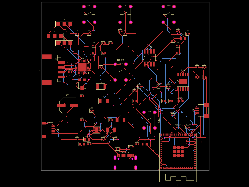 More from this authortscircuit/motor-controllerThis code defines a compact hardware layout with multiple integrated components such as microcontrollers, power regulators, sensors, connectors, and passive elements, all arranged on a PCB for a versatile electronic device.
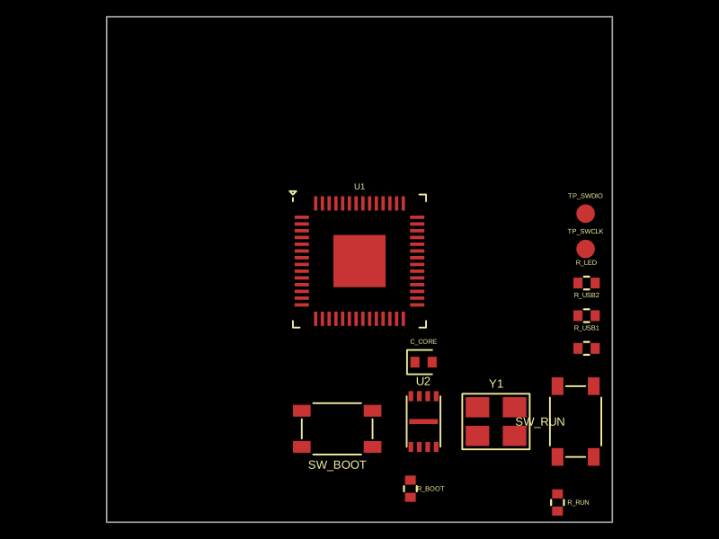 Similar packageMustafaMulla29/rp2040-chipThis code defines and maps a compact 30mm x 30mm PCB featuring an RP2040 microcontroller with integrated GPIO, power regulation, USB-C interface, QSPI flash memory, crystal oscillator, pushbuttons, test points, and associated routing traces.
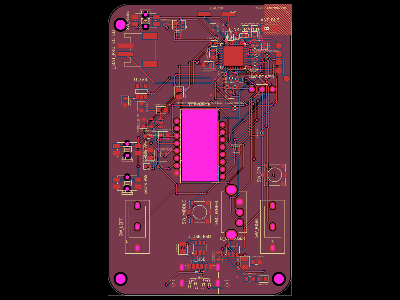 Discover something newMustafaMulla29/wireless-mouse-pcbA hardware component library defining footprints and 3D models for a 3.3 V regulator, RF antenna, switches, connectors, battery charger, and nRF52810 Bluetooth microcontroller.