muse/book-reading-clip-lamp
A 60‑mm ESP32‑S3 lamp-head PCB combining USB‑C battery charging/power regulation, OV5640 autofocus camera interfacing, I²S microphone and differential speaker audio, six‑LED boost-driven reading light, buttons, status indicators, and battery monitoring.
- Version
- 0.2.5
- License
- unset
- Stars
- 0
validation.txt
Schematic

LAMP CLIP HEAD REV B - VALIDATION RECORD
05 October 2026 | tscircuit0.0.2646 / CLI0.1.2237 / TypeScript5.9.3

STATUS: ROUTED ENGINEERING PROTOTYPE, NOT A MANUFACTURING RELEASE.
All results below are software checks. No board or camera sample has been tested.

Final checks (actual logs are in reports/)
 TypeScript                                   PASS
 Netlist                                      PASS; 0 errors / 0 warnings
 Schematic placement                          PASS
 PCB placement                                PASS; 0 errors,1 reviewed warning
 Full build circuit error records             0 (supplier/parts engine enabled)
 LED supplier/polarity/release audit            PASS; LED7=C965805, LED8=C965800
 Camera interface/ESP32 mapping audit          PASS
 Saved-routing guard                          PASS
 Gerber-derived shorts: top/bottom             PASS
 Gerber-derived shorts: inner1                 PASS
 Gerber-derived shorts: inner2                 PASS
 Clock and USB trace-length diagnostics        Completed; includes inferred branches, not timing qualification
 Routing-difficulty analysis                  Not completed; stalled, see report

Camera interface audit checks the compiled circuit against all24 camera
contacts plus2 hold-downs, DVP data ordering, level conversion, both supply
rails, preserved41 ESP32 module pads, exact JLC supplier IDs/model records,
all9 schematic sheets, and the64 passive designators in the BOM.

Physical design
 60 mm round, four copper layers, nominal1.6 mm; double-sided assembly.
 101 source components, 291 PCB traces, 366 vias.
 Normal routing target0.15 mm signals /0.15 mm copper clearance.
 All 366 vias verified:0.30 mm drill /0.45 mm copper; vias intersecting SMT pads need filled/capped DFM review.

Routing method
 Pipeline9 supplied initial paths. The changed layout was recaptured, then
 geometric rip-up and four-layer A* routing repaired conflicts with explicit
 through-via checks on all layers. Local widening restores nominal power
 widths where clearance permits; fine-pitch pad neck-downs remain. The final
 copper is saved with its full input guard. No error records or failing checks
 are suppressed. See saved-routing-provenance.json and routing-notes.txt.
 Via-size update: pads resized at existing centers; trace paths retained and
 full DRC plus all-layer shorts repeated. Board props and saved-route rules agree.
 Reviewed source corrections: 1 via relocations, 1 route replacements.
 No Rev A correction is reused without rechecking the new geometry.
 LED7/LED8 now use explicit JLCSearch imports with pin1 cathode / pin2 anode.
 Four trace endpoints were moved less than0.03 mm for their exact pads; the
 saved input was recaptured and its strict guard remains enabled.

Retained build warning types (38 records)
 pcb_component_missing_courtyard_warning: 7
 pcb_connector_not_in_accessible_orientation_warning: 1
 source_component_pins_underspecified_warning: 1
 source_no_ground_pin_defined_warning: 1
 source_no_power_pin_defined_warning: 5
 source_part_not_found_warning: 1
 source_pin_missing_trace_warning: 2
 source_refdes_convention_warning: 2
 supplier_footprint_mismatch_warning: 18

J2 is deliberately inward-facing for an internal flex, so the edge-access
warning is expected. Assembly needs clear latch/insertion access before
closing the head. It is not a user-accessible cable port. Other warnings
include unused USB SBU pins, missing courtyards on PCB wire/test pads and
incomplete electrical pin-role metadata and supplier footprint-match warnings.
These warnings remain for component/assembly review. Netlist checking is therefore not
a complete electrical-rule or drive-strength qualification.

Before fabrication
 Confirm the exact KLT camera drawing and a mating sample. Verify pin1/contact
 orientation, focus at reading distance, lens support, flex bend/latch space.
 Test external2.8 V/1.5 V sequencing, reset/powerdown/XCLK, autofocus firmware,
 DVP timing/clock skew, SCCB rise time, image stability and LDO temperature.
 U9 enable follows2.8 V but is not a power-good supervisor. Camera rails stay
 on while3.3 V is on; sensor powerdown does not independently cut the supplies.
 Review USB impedance, converter loops, return paths and copper widths with
 the chosen four-layer stack. Inner copper includes signal routing and pours,
 so continuous reference planes are not guaranteed. Check exact passive
 MPNs, capacitor DC bias, paste, all vias that intersect SMT pads, and JLC hold-down pad geometry.
 Existing prototype limits remain:100 mA default USB/wall-adapter input,
 obsolete INMP441-R7, unqualified antenna/acoustics/enclosure/temperature
 behavior. Read power-audit.txt and usb-power-policy.txt.

No manufacturing Gerber release, finished Muse firmware, physical assembly,
measured battery life, optical/audio/RF validation or regulatory test is claimed.
Muse needs custom board support, capture/question association and audio replies.
Camera sourcing is a direct manufacturer quote; stock, MOQ and price are unknown.
Related Packages
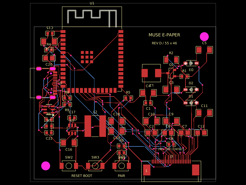 More from this authormuse/esp32-eink-displayA 55×46 mm two-layer ESP32-S3 e-paper controller board with USB‑C power/programming, buck regulation, FPC display connector, UC8179-style boost/charge-pump circuitry, ESD protection, controls, and routed passive components.
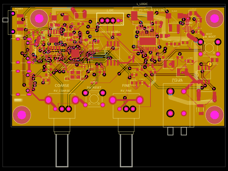 Discover something newastra/pd-power-supplyUSB-PD Power Supply with RP2040 controller