muse/book-reading-clip-lamp
A 60‑mm ESP32‑S3 lamp-head PCB combining USB‑C battery charging/power regulation, OV5640 autofocus camera interfacing, I²S microphone and differential speaker audio, six‑LED boost-driven reading light, buttons, status indicators, and battery monitoring.
- Version
- 0.2.5
- License
- unset
- Stars
- 0
power-audit.txt
Schematic

Independent electrical review — Lamp Clip head Rev B
Reviewed 2026-10-04: index.circuit.tsx and component wrappers.
This is a schematic/datasheet audit; electrical, thermal and EMC validation remain.

Highest-priority findings

1. Empty-battery boot starvation: fixed in the current source by SW3. The C&K switch has common pin 2; source connects pin 1 to SYS, pin 2 to SYS_EN, and pin 3 to GND. This disables the TPS63021 and the 3.3 V loads while charging remains active. Amplifier SD and LED CTRL pull-downs keep their SYS-powered loads disabled. The switch is charge-only, not complete battery isolation. The battery ADC divider can still inject a few microamps into the unpowered MCU; measure leakage and off-state 3.3 V during bring-up.

2. Self-powered USB sensing: the original missing monitor was addressed with a prototype 2N7002 detector. It does NOT establish USB compliance. Nexperia pinout: 1 gate, 2 source, 3 drain. The current 10k/100k gate network, 47k drain pull-up and 2k GPIO43 series resistor isolate 5 V and limit contention with the ROM UART TX output. However, the MOSFET threshold is variable; it does not meet the required 4.75 V valid / 4.35 V invalid thresholds. With C1 = 4.7 uF, the 110k bleed alone can hold VBUS for hundreds of milliseconds after unplug. Espressif requires detachment within 3 ms. Add a qualified threshold/discharge circuit and test timing before a final release. Firmware must invert the active-low detector, disable UART0 TX on GPIO43, and integrate the signal correctly with TinyUSB. Simply setting vbus_monitor_io generally assumes active-high presence.

3. USB suspend: the source implements the validated fix: GPIO3 / U1 pin 15 to BQ EN2, retaining the 10k pull-down. S3 strapping is latched at reset and the pin is usable as GPIO afterward; default eFuse settings ignore GPIO3 for JTAG source selection. BQ EN2/EN1 states are 00 USB100, 01 USB500, 10 ILIM, 11 suspend. Enter suspend by setting EN1 high before EN2 high. Resume by lowering EN2 before applying EN1 current policy. Retain output levels through MCU sleep and avoid the 10 state, which would allow approximately 957 mA. Charge-only or reset returns both pins low; behavior when a suspended host remains attached through these transitions requires system-level validation. USB100 is not USB suspend.

4. Wall-adapter charging: USB100 is the hardware default. GPIO21 may select USB500 only after host configuration requesting 500 mA. Wall adapters do not enumerate, so remain USB100. There is no CC current detector, BC1.2 detector or PD controller. The 500 mA ISET setting is a battery-charge ceiling, not a promise of battery current: system load consumes part of the input budget. A 2000 mAh pack needs well over 20 hours from near empty at USB100; test the complete charge cycle, timer behavior and fault indication. SW3 enables recovery without relying on successful MCU boot.

5. Battery temperature and low voltage: use a protected 1S, 4.2 V charge Li-ion/LiPo pack and a cell-mounted 10k Semitec 103AT-2 NTC. TI explicitly uses this part in its design example. Its R25 is 10k, B25/85 is 3435 K, and nominal resistance is 27.28k at 0 C and 4.160k at 50 C. The BQ nominal cold/hot resistance thresholds are 28k/4k. Do not claim a guaranteed 0–45 C charging window: verify the actual cell rating and adjust TS if necessary. Protection must cover overcharge, overdischarge, overcurrent and short circuit. TPS61165 requires at least 3.0 V VIN; firmware should stop the reading light before SYS falls below that, with graceful low-battery shutdown before pack protection opens.

Verified connections and remaining validation

BQ24074: BAT pins 2/3, OUT pins 10/11, IN pin 13, VSS/EP grounded, CE grounded, EN2 on GPIO3 with 10k pull-down, EN1 on GPIO21 with 100k pull-down. ISET 1.78k gives nominal 500 mA; ILIM 1.62k is within its allowed range but programmable-limit mode is not selected. ITERM floating uses the default threshold. TMR 46.4k gives approximately 6.2 hours nominal fast-charge timer before dynamic extension. Input 4.7 uF, BAT 10 uF and OUT 22 uF are within the stated ranges. TS requires the actual NTC; do not substitute a permanent fixed resistor in an assembled battery product.

CHG LED: current SYS-fed 1k/LED connection is appropriate and remains visible with the regulator off. TI describes LED use for CHG. Its maximum pin voltage is 7 V, maximum sink is 15 mA and VOL is specified at 5 mA; approximately 2.4 mA from SYS = 4.4 V is reasonable. CHG indicates initial charging and timer faults; it is not a complete battery fuel gauge.

TPS63021: supply, feedback-to-3.3 V, PS_SYNC ground, switching nodes and EP ground are correct. XFL4020-152MEC, 1.5 uH, has 4.1 A saturation rating at 10% inductance drop in the current Coilcraft data. Input 2x10 uF, output 3x22 uF and VINA 100 nF are sensible nominal values. Exact MLCC part numbers and capacitance after DC bias remain unverified. Route the power loop and bypasses locally with planes and thermal vias following TI's layout.

TPS61165: VIN 1 to SYS, CTRL 2 to PWM with 100k down, SW 3 to inductor/Schottky anode, GND 4, COMP 5 with 220 nF, FB 6 to sense. Six LEDs are in series; 13.3 ohm sets nominal 15.0 mA. LPS5030-103MRC is 10 uH, 1.4 A Isat at 10% drop and 1 A Irms at 20 C rise. The actual normal LED load has substantially lower peak current; validate fault/startup current versus the driver's maximum switch limit and inductor saturation. The 1 uF/50 V output capacitor is appropriate. The OVP threshold is 37–39 V and switch limit is at most 1.44 A; verify the 40 V diode margin against measured ringing before release. Hold CTRL high through startup before applying PWM to avoid unintended EasyScale entry.

D1 polarity: the JLCSearch C21353 MBR0540T1G import uses pin 1 = cathode and pin 2 = anode. The source connects pin 1 to LED_ANODE and pin 2 to LED_SW at rotation 180. Place the physical cathode band at imported pin 1 / LED_ANODE. This supersedes the earlier builtin SOD-123 numbering. Confirm assembly orientation against the onsemi package drawing; the boost switch loop still requires engineering review.

ESP32-S3: corrected WROOM-1U-N16R8 numbering, 3.3 V supply, EN 10k/1 uF and GPIO0 pull-up are coherent. GPIO35–37 stay unconnected because octal PSRAM uses them. USB GPIO19/20 are D-/D+; place 22 ohm series resistors near the MCU per Espressif. The external-antenna module requires a suitable U.FL antenna.

Camera Rev B: J2 mates the exact KLT-PAA40-OV5640-1B V1.0 ESP32 flex. U8 supplies 2.8 V analog/I/O/AF; U9 supplies external 1.5 V core, enabled from CAM2V8. U10/U11 translate outputs to3.3 V, U12 translates controls to2.8 V, U13 handles SCCB. Reset/clock default low and powerdown high. Camera rails stay on while3.3 V is enabled. Verify startup ramps, LDO dissipation and combined radio/camera transients on the bench; these are not measured results. Read camera-sourcing.txt for the complete pinout and startup notes.

Audio: INMP441 left slot, CHIPEN at 3.3 V, local 100 nF and SD 100k pull-down are coherent. The imported R7 ordering option is obsolete and is retained for this prototype only. MAX98357A DIN/BCLK/LRCLK and SYS bypassing are correct. Floating GAIN selects 9 dB. The 2k SD series resistor follows the manufacturer's protection recommendation when SYS can fall below 3.3 V; 100k pull-down disables the amplifier at reset. Supply left-slot audio or duplicate mono in both slots. Use 32-bit stereo slots with 24-bit microphone data and BCLK = 64 x Fs. The speaker is BTL between SPK+ and SPK-; neither wire may connect ground. Use an 8-ohm speaker with appropriate power rating and firmware volume limit.

Battery ADC: GPIO1 is ADC1_CH0. The 470k/470k divider gives 2.1 V from a 4.2 V pack, within the useful 12 dB calibrated range. Use ESP ADC calibration, averaging and approximately 120 ms settling for 5 RC. High source impedance and dynamic battery load need bench calibration; this is voltage monitoring, not an accurate state-of-charge gauge.

New footprint validation

PowerSwitch: C&K JS102011SAQN, JLC C221660. Manufacturer land pattern has three 1.2 x 2.5 mm pads at 2.5 mm pitch; two 0.9 mm NPTH locating holes are 6.8 mm apart and 2.75 mm below pad centers. Pin 2 is common; contacts are non-shorting. Lever exits toward -Y at rotation 0 and toward -X at rotation 270. A labeled schematic box preserves the actual numbering because the builtin SPDT symbol uses pin 1 as common.

VbusDetectorFet: Nexperia 2N7002,215, JLCSearch C65189 imported SOT23 land pattern, explicit G1/S2/D3 aliases. Both new wrappers compile and standalone placement returns zero errors and zero warnings. PCB preview build succeeds. These tests do not replace full-board routing and shorts checks.

Primary sources
https://www.ti.com/lit/ds/symlink/bq24074.pdf
https://www.ti.com/lit/ds/symlink/tps63021.pdf
https://www.ti.com/lit/ds/symlink/tps61165.pdf
https://www.coilcraft.com/getmedia/50632d43-da1b-4cdb-8ab4-3029cab51df3/xfl4020.pdf
https://www.coilcraft.com/getmedia/11b17d19-33b4-4b4c-8f03-09560f682bf1/lps5030.pdf
https://www.littelfuse.com/assetdocs/littelfuse-c-k-slide-js-series-datasheet?assetguid=aba42b08-0d2c-423b-813d-a2faa5a3bb14
https://datasheet.lcsc.com/datasheet/pdf/facc684708fd3febef29363c3f43748d.pdf (C&K drawing mirror; dimensions match current primary drawing)
https://assets.nexperia.com/documents/data-sheet/2N7002.pdf
https://www.onsemi.com/pdf/datasheet/mbr0540t1-d.pdf
https://docs.espressif.com/projects/esp-idf/en/v5.5/esp32s3/api-reference/peripherals/usb_device.html
https://www.espressif.com/sites/default/files/documentation/esp32-s3-wroom-1_wroom-1u_datasheet_en.pdf
https://www.analog.com/media/en/technical-documentation/data-sheets/MAX98357A-MAX98357B.pdf
https://semiteckorea.com/wp-content/uploads/2019/06/SEMITEC-Product-catalog-5-mb.pdf

Final footprint/routing implementation notes
The WROOM exposed pad uses nine original solder windows joined by four mask-covered ground-copper bridges. This creates one connected pin41 copper region; no new paste windows are added. Thermal vias on BQ24074, TPS63021 and MAX98357 are offset 0.2 mm inside their pads and connected by explicit short tracks to the GND planes. Switching nets BUCK_L1/L2 request 0.8 mm nominal copper; speaker/LED switch nets request 0.4 mm. Widths may neck down near pads and still need current/loop review. Final tool results are in validation.txt.

JLCSearch import update
All U1-U7 ICs/modules, Q1 and D1 now use local JLCSearch/EasyEDA imports.
The BQ24074 and TPS63021 no longer use the earlier hand-built QFN lands.
The TPS63021 import retains its comb-shaped exposed pad. INMP441 retains
the imported copper, with the 0.5 mm board acoustic drill (TDK recommends 0.5–1.0 mm) and a ground tab.
Component identities, exact supplier IDs and modifications are recorded in
component-provenance.csv. Imported symbol pin names are corrected from
manufacturer datasheets where needed. Thermal vias in exposed pads require
a filled/capped via-in-pad process, or a reviewed redesign before manufacture.
Related Packages
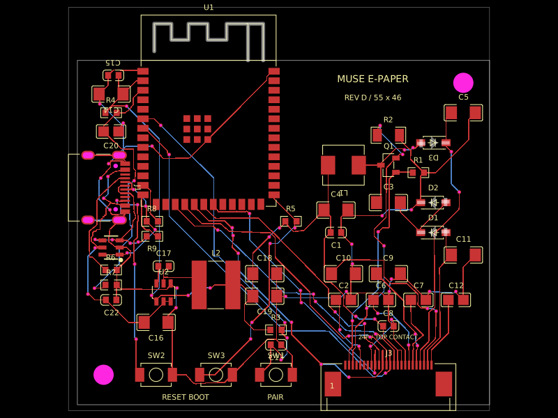 More from this authormuse/esp32-eink-displayA 55×46 mm two-layer ESP32-S3 e-paper controller board with USB‑C power/programming, buck regulation, FPC display connector, UC8179-style boost/charge-pump circuitry, ESD protection, controls, and routed passive components.
 Discover something newastra/pd-power-supplyUSB-PD Power Supply with RP2040 controller