README.md
# Mini MP3 Player — Rev B, headphones only

The native tscircuit **3D** viewer now includes the enclosure, LiPo beneath the PCB, three-wire JST harness, four labeled captive button caps, and small flush LED windows. Use the visible **Assembled / Open case / Exploded / PCB only** buttons. Assembly modes start in 3D; the Schematic button opens the multi-sheet drawing. The compact enclosure is 88 × 68 × 21.5 mm. These are CAD-only subassemblies; PCB geometry and electrical nets are unchanged. See `mechanical/README.md` for dimensions and prototype limitations. Run `bun run models` to regenerate models and `bun run build:site` to rebuild the viewer with its selector.

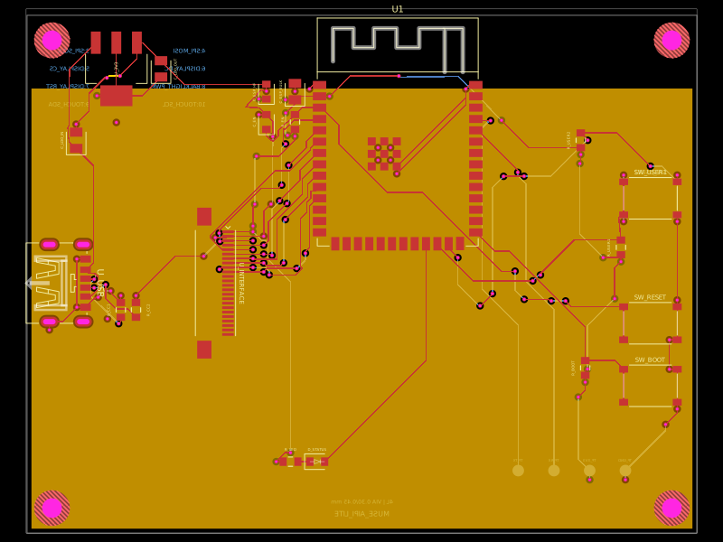
An 82 × 62 mm, two-layer tscircuit design with top-side component assembly. CH32V203C8T6 reads microSD files and streams compressed audio to a VS1003B-L. The VS1003 performs decoding and drives capacitively coupled, ground-referenced stereo headphones.

The display, speaker and speaker amplifier are omitted. Four pushbuttons provide play/pause, previous, next and volume mode. Included prototype firmware behavior is: tap VOL to toggle volume mode; PREV/NEXT then lower/raise volume. Tap VOL again to restore track navigation. Blink the green LED while volume mode is active. Firmware is compiled and host-tested; physical playback testing is pending. A slide switch disconnects the system while leaving battery charging available. Red indicates charging; green is firmware controlled. Reset remains available at the debug pad, with no separate reset pushbutton.

Rev B removes 12 fitted components from Rev A. The 82 × 62 mm outline is retained for comfortable button spacing, easy routing and debugging. The decoder occupies the space freed by the speaker, increasing separation from the MCU.

## Open and build

```sh
bun install --frozen-lockfile
bun run typecheck
bun run build
bun run dev
# Static interactive viewer:
bunx tsci build index.circuit.tsx --site
```

`index.circuit.tsx` defines functional placement and automatic routing. The validated autorouter result is saved in `routing/autorouter-result.json`; the 0.30/0.45 mm via reroute includes three small via adjustments and local UART/ground trace clearance repairs, recorded in validation/via-clearance-repairs.json. The replay checks the complete routing input and rejects changed placement, wiring or rules. To reroute an edited board, remove `algorithmFn:savedAutorouting` from the board autorouter settings, build, validate and refresh the saved result. The cache preserves the normal signals generated by the autorouter; it does not disable DRC. The crystal loops are explicitly routed; ordinary signals use the autorouter. `design.ts` contains physical pin-to-net assignments and passive values. Imported component files include LCSC identifiers and footprints. `schAutoLayoutEnabled` remains enabled; schematic symbol positions are not manually arranged. Spacing margins help the automatic layout avoid label collisions. Small bottom-layer copper keepouts below selected top pads keep unfilled routing vias clear of solder pads; they do not create board cutouts.

## Schematic sheets

The schematic uses four automatically arranged sheets: **01 USB-C, Battery & Power**, **02 MCU & Programming**, **03 MP3 Decoder & Headphones**, and **04 microSD & Buttons**. Functional sections group Power, MCU, Debug, Decoder, Audio, Storage, and Controls within these sheets. Use the schematic viewer sheet selector to switch pages. Each sheet includes explanatory notes naming the relevant components, supply rails, interfaces and user behavior. Component symbol placement remains automatic.

## Electrical design

| Block | Device / part | Design detail |
|---|---|---|
| MCU | CH32V203C8T6 / C3001172 | 8 MHz crystal; all five supply groups decoupled; reset and boot straps |
| Decoder | VS1003B-L / C9921 | 12.288 MHz crystal; separate SCI/SDI selects; DREQ; reset; boot/test straps |
| Charger | BQ24074RGTR / C54313 | Power path, nominal 300 mA charging, 500 mA input mode, battery NTC |
| Logic | ME6211C33M5G-N / C82942 | 3.3 V MCU, card and decoder I/O |
| Decoder core | ME6211A25M3G-N / C2835782 | 2.5 V |
| Decoder analog | ME6219C27M5G / C236645 | **2.7 V**, within the VS1003 2.6–2.85 V analog range |
| Headphones | PJ-320D / C431535 | TRS-compatible tip/ring/sleeve wiring; 220 µF per channel |

The requested 3.3 V analog supply was corrected: 3.3 V exceeds the VS1003 analog operating range. Decoder GBUF is **not** headphone ground and is never directly grounded. Each audio output and GBUF has the manufacturer-recommended series RC stabilization network. Both headphone contacts in the sleeve region are grounded, and the audio outputs are AC coupled.

Battery input J2 is a **three-wire protected 1S, 4.2 V Li-ion/LiPo pack**, suggested capacity at least 600 mAh: pin 1 BAT+, pin 2 10 kΩ NTC, pin 3 BAT−/GND. Verify connector polarity against the actual pack; JST wiring is not universally standardized. The NTC must be thermally coupled to the cell. An absent NTC inhibits charging. Cell protection is required in the pack; the charger is not a substitute for discharge/short-circuit protection. No battery is part of the assembled PCB BOM.

Q1 switches the system load so the slide switch carries only gate current. Q2 switches the battery divider to avoid powering the ADC through its protection diode when the system is off. The ADC divider is 100 kΩ / 100 kΩ with 100 nF filtering. Firmware stops playback after three readings below nominal 3.55 V under load, before the 3.3 V regulator loses useful headroom. Use a long ADC acquisition time and calibrate the divider/reference.

USB-C is for power/charging only. Both CC pins have independent 5.1 kΩ pull-downs. R37 pulls charger EN1 high through 10 kΩ while EN2 is grounded, selecting USB500 mode; this local strap keeps a routing via away from the QFN pad. The 10 kΩ resistor dominates the approximately 285 kΩ internal EN1 pull-down. USB data pins are unused. The charger prioritizes the system and reduces charging current when its input budget or temperature requires it. Charging time therefore depends on playback load and thermal conditions.

## Programming and firmware contract

Connect a WCH-Link in RISC-V mode to TP1 GND, TP2 3.3 V reference, TP3 PA13/SWDIO and TP4 PA14/SWCLK. TP5 exposes NRST. Use the board's power supply; avoid backfeeding it from the programmer. TP6/TP7 expose PA9 TX and PA10 RX for 3.3 V UART diagnostics. TP8 exposes BOOT0; its default pull-down selects user flash. BOOT1 is also pulled down.

TP16 is the charger's open-drain PGOOD output. Add an external 10 kΩ pull-up to TP2 when measuring its logic state; it has no onboard pull-up. The debug pads accept soldered leads or a pogo fixture rather than a fitted header.

| Function | CH32 pin / peripheral |
|---|---|
| microSD | SPI1: PA5 SCK, PA6 MISO, PA7 MOSI; PA4 CS |
| VS1003 | SPI2: PB13 SCK, PB14 MISO, PB15 MOSI |
| Decoder control | PB12 XCS, PB9 XDCS, PB8 XRESET, PA8 DREQ |
| Buttons, active low | PA1 play, PA2 previous, PA3 next, PB0 volume mode |
| Status LED | PB11, low lights |
| Battery measurement | PA0/ADC0; battery voltage is twice ADC input voltage |

Prototype playback firmware, source, ELF/BIN/HEX and host tests are included under `firmware/`. See `firmware/README.md` for flashing and usage. It implements read-only FAT16/FAT32 root-file playback, VS1003 streaming, all four buttons, volume mode, error indication and a nominal 3.55 V low-battery playback stop. It is not hardware-tested. Start with `PROTOTYPE.md` for the fabrication package and first-board acceptance procedure.

## Bring-up

1. Inspect assembly orientation, bridges and polarized C43/C44. Verify battery polarity before connecting a pack.
2. With no battery, use current-limited USB 5 V. Check USB5V, SYS_RAW and switched SYS. With the switch off, verify SYS and BAT_ADC fall close to zero.
3. Switch on and measure TP2 = 3.3 V, TP12 = 2.5 V and TP13 = 2.7 V. Check rail ripple and regulator temperature under load.
4. Attach WCH-Link and flash the included prototype firmware and inspect UART diagnostics. Test all four buttons, both LEDs and battery ADC. TP5 can be momentarily connected to ground to reset the MCU.
5. Verify oscillator startup, SD initialization and card block reads. Verify VS1003 reset/DREQ and SCI register reads before streaming a known MP3.
6. Test headphones at low volume. Confirm negligible DC across the headphones and check both stereo channels and volume control.
7. Connect a protected pack with its NTC. Measure actual charge current, termination and temperature. Repeat playback/charge and low-battery tests.

Top assembly does not mean a single copper layer: bottom copper and plated vias provide routing and ground return. Connector/card mechanical clearances must be checked with the chosen enclosure. The electrolytics and connectors set the enclosure height. An enclosure inspection model is included; physical fit and print qualification are pending.

## Fabrication files

After a successful build, `bun run release` checks the electrical assertions and refuses export if any DRC errors remain. It produces a Gerber/drill archive, grouped JLCPCB BOM and top-side pick-and-place CSV under `manufacturing/`, plus schematic, PCB and assembly SVGs under `dist/index/`. Use a two-layer, 1.6 mm FR-4 board with 1 oz copper. Minimum via drill is 0.30 mm and minimum copper pad diameter is 0.45 mm (0.075 mm nominal radial annulus). The nominal signal width is 0.18 mm and power nets use 0.3 mm routing; ground pours are on both faces. The assembler should review connector orientation and polarity against the assembly drawing before production.

**Generate fabrication files with `bun run release`.** Its stencil stage supplies apertures missing from the installed library's pill-pad export, excludes test pads/fiducials and bottom paste, and windows the charger thermal pad to 58.5% coverage. Ordinary rectangular apertures use 90% of pad width and height; the rounded IC pads use inscribed rectangles. A 0.10–0.12 mm stencil is the starting specification for the assembler's process review. `manufacturing/release.circuit.json` retains the same copper and connectivity with these explicit paste apertures.

The battery, microSD card, headphones, programmer and enclosure are external items. Fabrication exports do not imply that a prototype has been assembled or bench tested.

## Source references

- [WCH official CH32V20x reference designs and SDK](https://github.com/openwch/ch32v20x)
- [Official CH32V203C8T6 reference schematic](https://github.com/openwch/ch32v20x/blob/main/SCHPCB/CH32V203C-R0/SCH_PCB/CH32V203C8T6-R0.pdf)
- [VS1003 datasheet](https://www.vlsi.fi/fileadmin/datasheets/vs1003.pdf)
- [BQ24074 datasheet](https://www.ti.com/lit/ds/symlink/bq24074.pdf)

LCSC/JLCPCB component codes identify procurement candidates. Assembly availability and stock must be checked at order time. See `VALIDATION.md` for the actual verification status; a rendered board image alone is not evidence of manufacturing readiness.