krishnax12/watchy-eink-smartwatch
Unfinished prototype (not production-ready): 4 native DRC errors, 2 display-flex intersections, and missing antenna radiator copper remain
- Version
- 1.2.7
- License
- MIT
- Stars
- 1
scripts/usb-assembly.test.ts
import { expect, test } from "bun:test";
import type { AnyCircuitElement } from "circuit-json";
import {
	applyToPoint,
	compose,
	rotateDEG,
	translate,
} from "transformation-matrix";
import { BOARD_THICKNESS_MM } from "../pcb/board-stackup";

test("USB mounting rows and solder contacts register with the native footprint", async () => {
	const circuit: AnyCircuitElement[] = await Bun.file(
		"dist/index/circuit.json",
	).json();
	const connector = circuit.find(
		(element) =>
			element.type === "cad_component" &&
			element.model_step_url?.endsWith("/EasyEDA_C91146_U_F_M5DD_Y_L.step"),
	);
	if (!connector || connector.type !== "cad_component") {
		throw new Error("Missing USB model");
	}
	const origin = connector.model_origin_position;
	if (!origin) throw new Error("Missing USB model origin");
	const rotation = connector.rotation;
	if (!rotation) throw new Error("Missing USB model rotation");
	expect(rotation.x).toBe(0);
	expect(rotation.y).toBe(0);
	expect(rotation.z).toBe(270);
	expect(origin.z).toBe(0);
	expect(connector.position.z).toBeCloseTo(BOARD_THICKNESS_MM / 2, 6);
	const modelToBoard = compose(
		translate(connector.position.x, connector.position.y),
		rotateDEG(rotation.z),
		translate(-origin.x, -origin.y),
	);

	// Datums measured from the unmodified C91146 STEP. Both tab rows are
	// registered symmetrically; residual row-spacing differences stay visible.
	const mountingTabs = [
		{ pin: "pin6", x: -3.625, y: 0 },
		{ pin: "pin9", x: 3.625, y: 0 },
		{ pin: "pin8", x: 2.425, y: -2.715 },
		{ pin: "pin7", x: -2.425, y: -2.715 },
	];
	for (const tab of mountingTabs) {
		const hole = circuit.find(
			(element) =>
				element.type === "pcb_plated_hole" &&
				element.pcb_component_id === connector.pcb_component_id &&
				element.port_hints?.includes(tab.pin),
		);
		if (!hole || hole.type !== "pcb_plated_hole") {
			throw new Error(`Missing USB mounting hole ${tab.pin}`);
		}
		const center = applyToPoint(modelToBoard, tab);
		expect(Math.abs(center.x - hole.x)).toBeLessThan(0.05);
		expect(Math.abs(center.y - hole.y)).toBeLessThan(0.05);
	}

	// All five flat solder-contact undersides must land inside their copper
	// pads, not just share a visually similar shell outline. STEP plane is Z=0.
	for (const contact of [
		{ pin: "pin1", x: 1.3 },
		{ pin: "pin2", x: 0.65 },
		{ pin: "pin3", x: 0 },
		{ pin: "pin4", x: -0.65 },
		{ pin: "pin5", x: -1.3 },
	]) {
		const pad = circuit.find(
			(element) =>
				element.type === "pcb_smtpad" &&
				element.pcb_component_id === connector.pcb_component_id &&
				element.port_hints?.includes(contact.pin),
		);
		if (!pad || pad.type !== "pcb_smtpad" || pad.shape !== "rect") {
			throw new Error(`Missing USB signal pad ${contact.pin}`);
		}
		for (const x of [contact.x - 0.2, contact.x + 0.2]) {
			for (const y of [-2.89, -2.315]) {
				const corner = applyToPoint(modelToBoard, { x, y });
				expect(Math.abs(corner.x - pad.x)).toBeLessThan(pad.width / 2);
				expect(Math.abs(corner.y - pad.y)).toBeLessThan(pad.height / 2);
			}
		}
	}
});
Related Packages
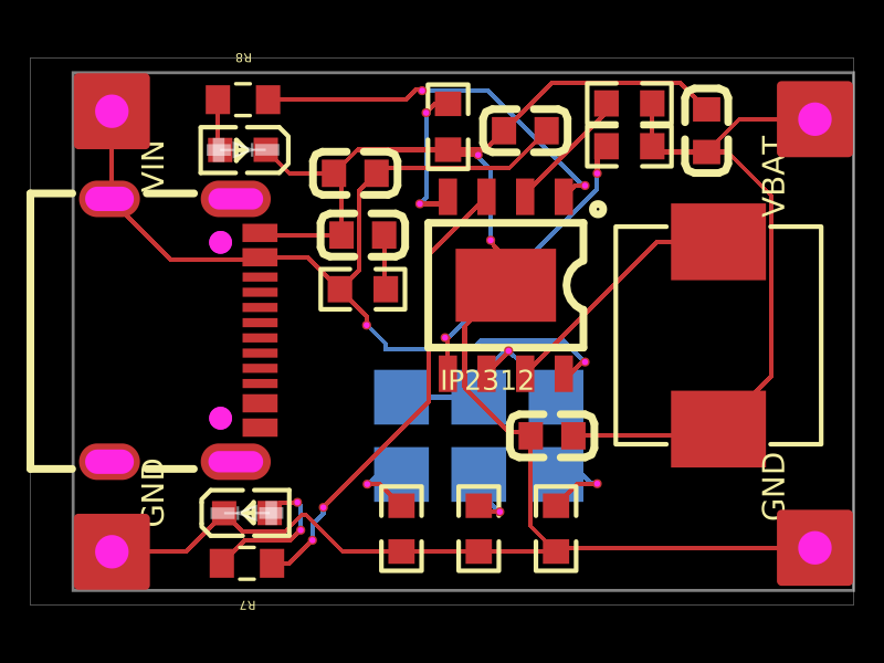 More from this authorkrishnax12/ip2312-fast-charging-moduleThis design implements a compact PCB with a USB-C input port, IP2312 battery charger IC, associated passive components (capacitors, resistors, inductor), output terminals for BAT and GND, and status indicator LEDs, facilitating fast lithium battery charging.
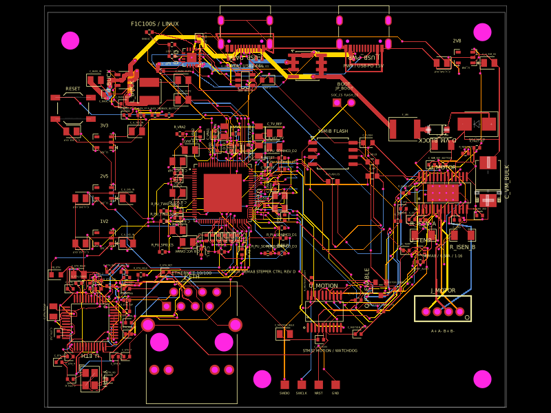 Similar packageshibosoftwaredev/f1c100s-linux-nema8-stepper-controllerRestores component part numbers and CAD models, removes test-point 3D bodies, and validates that solder paste exists only on top-side SMT pads without altering copper or DRC.
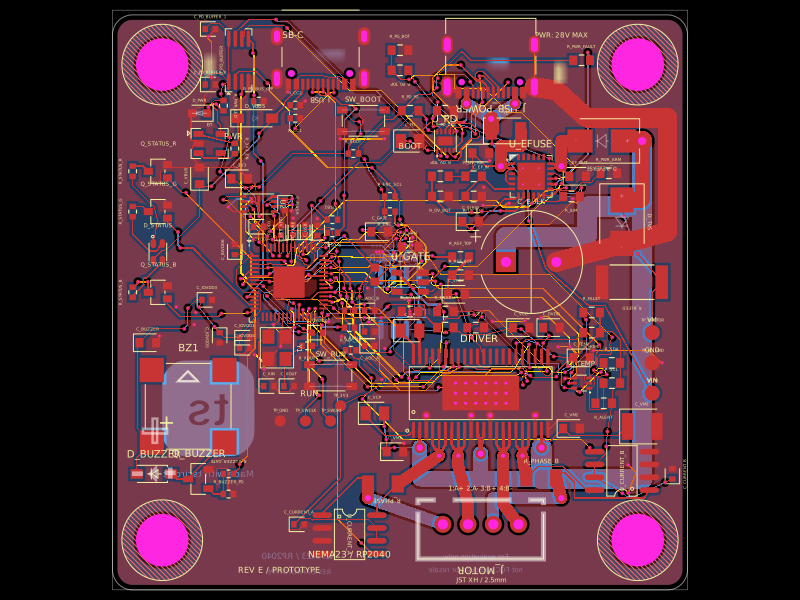 Discover something newimrishabh18/nema-23-stepper-controllerA 57 mm four-layer RP2040 NEMA23 stepper-controller PCB with USB‑C/USB‑PD power input, protected motor rail, DRV8452 dual-winding driver, bidirectional current sensing, temperature/enable interlock, optional magnetic encoder, RGB LED and buzzer status indicators, and motor/test connectors.