krishnax12/watchy-eink-smartwatch
Unfinished prototype (not production-ready): 4 native DRC errors, 2 display-flex intersections, and missing antenna radiator copper remain
- Version
- 1.2.7
- License
- MIT
- Stars
- 1
schematic/EpaperInterfaceSection.tsx
import { AO3400A } from "../imports/AO3400A";
import { Display } from "../imports/Display";
import { FPC24 } from "../imports/FPC24";
import { MBR0530 } from "../imports/MBR0530";
import { SRN4018_47uH } from "../imports/SRN4018_47uH";
import { schematicSections, schematicSheets } from "./config";

export const EpaperInterfaceComponents = () => (
	<>
		<AO3400A
			name="Q3"
			pcbX={11.24}
			pcbY={-13.77}
			pcbRotation={90}
			schSectionName={schematicSections.epaperBias}
			schSheetName={schematicSheets.epaperDriver}
		/>
		<SRN4018_47uH
			name="L2"
			pcbX={-10.41}
			pcbY={-13.22}
			pcbRotation={90}
			schSectionName={schematicSections.epaperBias}
			schSheetName={schematicSheets.epaperDriver}
		/>
		<MBR0530
			name="D5"
			pcbX={-11.05}
			pcbY={-7.16}
			pcbRotation={90}
			schSectionName={schematicSections.epaperBias}
			schSheetName={schematicSheets.epaperDriver}
		/>
		<resistor
			name="R17"
			resistance="2.2Ω"
			footprint="0402"
			pcbX={4.7}
			pcbY={-2.4}
			pcbRotation={90}
			schSectionName={schematicSections.epaperBias}
			schSheetName={schematicSheets.epaperDriver}
		/>
		<MBR0530
			name="D4"
			pcbX={-13.35}
			pcbY={-7.16}
			pcbRotation={90}
			schSectionName={schematicSections.epaperBias}
			schSheetName={schematicSheets.epaperDriver}
		/>
		<capacitor
			name="C21"
			capacitance="4.7uF"
			maxVoltageRating="50V"
			schShowRatings
			footprint="0603"
			pcbX={-11.18}
			pcbY={-10.24}
			schSectionName={schematicSections.epaperBias}
			schSheetName={schematicSheets.epaperDriver}
		/>
		<capacitor
			name="C20"
			capacitance="4.7uF"
			maxVoltageRating="50V"
			schShowRatings
			footprint="0603"
			pcbX={-11.18}
			pcbY={-16.2}
			schSectionName={schematicSections.epaperBias}
			schSheetName={schematicSheets.epaperDriver}
		/>
		<resistor
			name="R16"
			resistance="1MΩ"
			footprint="0402"
			pcbX={5.7}
			pcbY={-2.4}
			pcbRotation={270}
			schSectionName={schematicSections.epaperBias}
			schSheetName={schematicSheets.epaperDriver}
		/>
		<MBR0530
			name="D3"
			pcbX={-15.65}
			pcbY={-7.16}
			pcbRotation={270}
			schSectionName={schematicSections.epaperBias}
			schSheetName={schematicSheets.epaperDriver}
		/>
		<FPC24
			name="J3"
			pcbX={0.05}
			pcbY={-6.39}
			schSectionName={schematicSections.epaper}
			schSheetName={schematicSheets.epaper}
			noConnect={["pin1", "pin4", "pin6", "pin7", "pin19", "pin25"]}
		>
			<Display />
		</FPC24>
		<capacitor
			name="C29"
			capacitance="1uF"
			maxVoltageRating="50V"
			schShowRatings
			footprint="0402"
			pcbX={-5.96}
			pcbY={-2.4}
			pcbRotation={90}
			schSectionName={schematicSections.epaperBias}
			schSheetName={schematicSheets.epaperDriver}
		/>
		<capacitor
			name="C25"
			capacitance="1uF"
			maxVoltageRating="50V"
			schShowRatings
			footprint="0402"
			pcbX={-2.96}
			pcbY={-2.4}
			pcbRotation={270}
			schSectionName={schematicSections.epaperBias}
			schSheetName={schematicSheets.epaperDriver}
		/>
		<capacitor
			name="C27"
			capacitance="1uF"
			maxVoltageRating="50V"
			schShowRatings
			footprint="0402"
			pcbX={0.65}
			pcbY={-2.4}
			pcbRotation={270}
			schSectionName={schematicSections.epaperBias}
			schSheetName={schematicSheets.epaperDriver}
		/>
		<capacitor
			name="C22"
			capacitance="1uF"
			maxVoltageRating="50V"
			schShowRatings
			footprint="0402"
			pcbX={-3.96}
			pcbY={-2.4}
			pcbRotation={270}
			schSectionName={schematicSections.epaperBias}
			schSheetName={schematicSheets.epaperDriver}
		/>
		<capacitor
			name="C23"
			capacitance="1uF"
			maxVoltageRating="50V"
			schShowRatings
			footprint="0402"
			pcbX={3.7}
			pcbY={-2.4}
			pcbRotation={270}
			schSectionName={schematicSections.epaperBias}
			schSheetName={schematicSheets.epaperDriver}
		/>
		<capacitor
			name="C24"
			capacitance="1uF"
			maxVoltageRating="50V"
			schShowRatings
			footprint="0402"
			pcbX={-1.96}
			pcbY={-2.4}
			pcbRotation={270}
			schSectionName={schematicSections.epaperBias}
			schSheetName={schematicSheets.epaperDriver}
		/>
		<capacitor
			name="C28"
			capacitance="1uF"
			maxVoltageRating="50V"
			schShowRatings
			footprint="0402"
			pcbX={-0.96}
			pcbY={-2.4}
			pcbRotation={270}
			schSectionName={schematicSections.epaperBias}
			schSheetName={schematicSheets.epaperDriver}
		/>
		<capacitor
			name="C26"
			capacitance="1uF"
			maxVoltageRating="50V"
			schShowRatings
			footprint="0402"
			pcbX={-4.96}
			pcbY={-2.4}
			pcbRotation={270}
			schSectionName={schematicSections.epaperBias}
			schSheetName={schematicSheets.epaperDriver}
		/>
		<resistor
			name="R19"
			resistance="100kΩ"
			footprint="0402"
			pcbX={2.7}
			pcbY={-2.4}
			pcbRotation={90}
			schSectionName={schematicSections.epaperBias}
			schSheetName={schematicSheets.epaperDriver}
		/>
	</>
);

export const EpaperInterfaceTraces = () => (
	<>
		<trace from=".Q3 > .pin1" to="net.GDR" />
		<trace from=".R16 > .pin1" to="net.GDR" />
		<trace from=".J3 > .pin2" to="net.GDR" />
		<trace from=".Q3 > .pin2" to="net.RESE" />
		<trace from=".R17 > .pin2" to="net.RESE" />
		<trace from=".J3 > .pin3" to="net.RESE" />
		<trace from=".Q3 > .pin3" to="net.EINK_BOOST_SW" />
		<trace from=".L2 > .pin1" to="net.EINK_BOOST_SW" />
		<trace from=".D5 > .pin2" to="net.EINK_BOOST_SW" />
		<trace from=".C21 > .pin2" to="net.EINK_BOOST_SW" />
		<trace from=".L2 > .pin2" to="net.P3V3" />
		<trace from=".C20 > .pin1" to="net.P3V3" />
		<trace from=".J3 > .pin15" to="net.P3V3" />
		<trace from=".J3 > .pin16" to="net.P3V3" />
		<trace from=".C28 > .pin1" to="net.P3V3" />
		<trace from=".R19 > .pin1" to="net.P3V3" />
		<trace from=".D5 > .pin1" to="net.PREVGH" />
		<trace from=".J3 > .pin21" to="net.PREVGH" />
		<trace from=".C22 > .pin1" to="net.PREVGH" />
		<trace from=".R17 > .pin1" to="net.GND" />
		<trace from=".D4 > .pin1" to="net.GND" />
		<trace from=".C20 > .pin2" to="net.GND" />
		<trace from=".R16 > .pin2" to="net.GND" />
		<trace from=".J3 > .pin8" to="net.GND" />
		<trace from=".J3 > .pin17" to="net.GND" />
		<trace from=".C29 > .pin1" to="net.GND" />
		<trace from=".C25 > .pin2" to="net.GND" />
		<trace from=".C27 > .pin2" to="net.GND" />
		<trace from=".C22 > .pin2" to="net.GND" />
		<trace from=".C23 > .pin2" to="net.GND" />
		<trace from=".C24 > .pin2" to="net.GND" />
		<trace from=".C28 > .pin2" to="net.GND" />
		<trace from=".C26 > .pin2" to="net.GND" />
		<trace from=".D4 > .pin2" to="net.EINK_VGL_PUMP" />
		<trace from=".C21 > .pin1" to="net.EINK_VGL_PUMP" />
		<trace from=".D3 > .pin1" to="net.EINK_VGL_PUMP" />
		<trace from=".D3 > .pin2" to="net.PREVGL" />
		<trace from=".J3 > .pin23" to="net.PREVGL" />
		<trace from=".C29 > .pin2" to="net.PREVGL" />
		<trace from=".J3 > .pin5" to="net.EINK_VCOM" />
		<trace from=".C23 > .pin1" to="net.EINK_VCOM" />
		<trace from=".J3 > .pin9" to="net.BUSY" />
		<trace from=".J3 > .pin10" to="net.RES" />
		<trace from=".R19 > .pin2" to="net.RES" />
		<trace from=".J3 > .pin11" to="net.DC" />
		<trace from=".J3 > .pin12" to="net.CS" />
		<trace from=".J3 > .pin13" to="net.SCK" />
		<trace from=".J3 > .pin14" to="net.MOSI" />
		<trace from=".J3 > .pin18" to="net.EINK_CAP1" />
		<trace from=".C24 > .pin1" to="net.EINK_CAP1" />
		<trace from=".J3 > .pin20" to="net.EINK_CAP2" />
		<trace from=".C25 > .pin1" to="net.EINK_CAP2" />
		<trace from=".J3 > .pin22" to="net.EINK_CAP3" />
		<trace from=".C26 > .pin1" to="net.EINK_CAP3" />
		<trace from=".J3 > .pin24" to="net.EINK_CAP4" />
		<trace from=".C27 > .pin1" to="net.EINK_CAP4" />
	</>
);
Related Packages
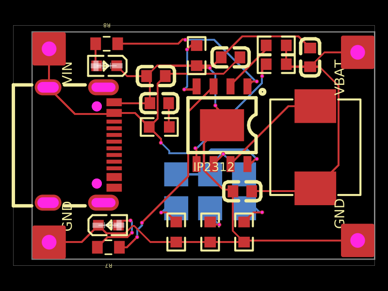 More from this authorkrishnax12/ip2312-fast-charging-moduleThis design implements a compact PCB with a USB-C input port, IP2312 battery charger IC, associated passive components (capacitors, resistors, inductor), output terminals for BAT and GND, and status indicator LEDs, facilitating fast lithium battery charging.
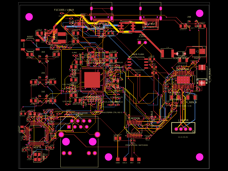 Similar packageshibosoftwaredev/f1c100s-linux-nema8-stepper-controllerRestores component part numbers and CAD models, removes test-point 3D bodies, and validates that solder paste exists only on top-side SMT pads without altering copper or DRC.
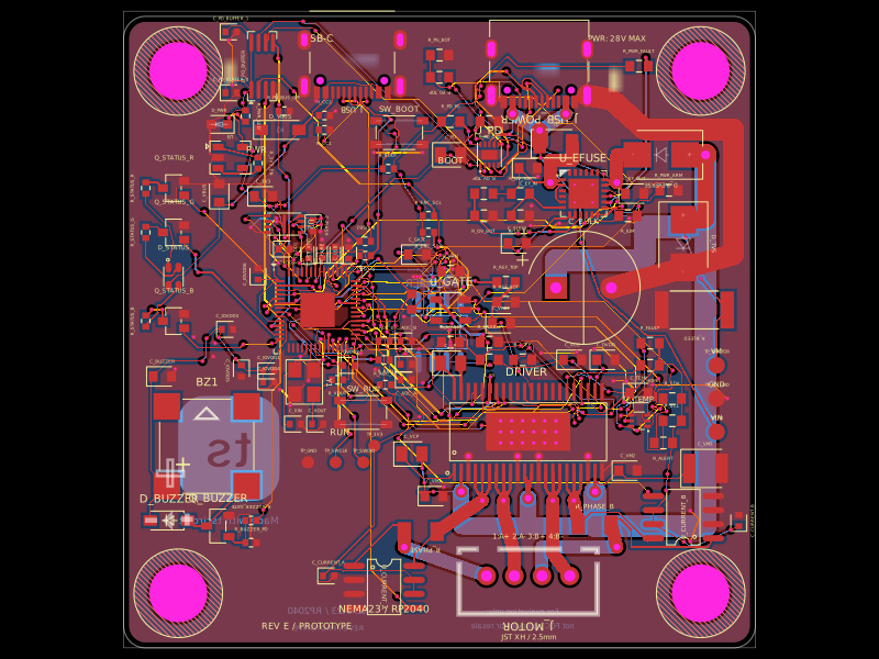 Discover something newimrishabh18/nema-23-stepper-controllerA 57 mm four-layer RP2040 NEMA23 stepper-controller PCB with USB‑C/USB‑PD power input, protected motor rail, DRV8452 dual-winding driver, bidirectional current sensing, temperature/enable interlock, optional magnetic encoder, RGB LED and buzzer status indicators, and motor/test connectors.