krishnax12/watchy-eink-smartwatch
Unfinished prototype (not production-ready): 4 native DRC errors, 2 display-flex intersections, and missing antenna radiator copper remain
- Version
- 1.2.7
- License
- MIT
- Stars
- 1
reports/production-status.json
{
	"productionReady": false,
	"published": false,
	"upstreamActions": "No PRs or issues created, as requested.",
	"dependencies": {
		"tscircuit": "0.0.2727",
		"core": "0.0.2048",
		"checks": "0.0.233"
	},
	"scope": "Released-tscircuit build with no patched dependencies, manual schematic placement, authored signal paths, or disabled checks. Physical PCB component coordinates are explicit and include clearance corrections; PCB placement is not claimed to be fully automatic.",
	"electricalBuild": {
		"nets": 53,
		"connectedPins": 237,
		"traces": 184,
		"vias": 166,
		"nativeErrors": 4,
		"independentRoutingConstraintErrors": 3,
		"routingConstraintCheck": [
			"RF_ANT violates the required top-only, no-via routing rule",
			"XTAL_40M_FB violates the required top-only, no-via routing rule",
			"XTAL_40M_OUT violates the required top-only, no-via routing rule"
		],
		"schematicWarnings": 4,
		"pcbWarnings": 34,
		"rootPlacementErrors": 0,
		"routingSkipped": false,
		"errorCounts": {
			"pcb_trace_too_long_error": 1,
			"pcb_trace_error": 2,
			"pcb_placement_error": 1
		},
		"nativeErrorMessages": [
			"PCB trace is 11.54mm long, exceeding the 10mm maximum",
			"PCB trace uses 2 vias, exceeding the 0 maximum",
			"PCB trace uses 2 vias, exceeding the 0 maximum",
			"Via pcb_via_19 violates copper-to-board-edge clearance (measured 0.158mm, required 0.200mm)"
		]
	},
	"referenceValueAudit": {
		"checked": 52,
		"mismatches": 0,
		"scope": "50 R/C/L quantities and two crystal frequencies against official v3 schematic. Not exact MPN, tolerance or crystal load-capacitance certification.",
		"fixed": "Ten e-paper capacitor strings now use separate native capacitance and 50 V rating properties; compiled quantities are in microfarads, not farads."
	},
	"nativeCopper": {
		"topGroundRegions": 11,
		"bottomGroundRegions": 2,
		"solderMaskCovered": true,
		"antennaKeepoutLayers": [
			"top",
			"bottom"
		],
		"antennaKeepoutExcludedComponents": [
			"AE1"
		],
		"authoredSignalGeometry": false
	},
	"viaGeometryMm": {
		"scope": "Current completed native autorouter output. Fabrication capability is not qualified.",
		"drill": 0.2,
		"pad": 0.35,
		"manufacturerCapabilityVerified": false
	},
	"frameworkLimitations": [
		"Current generated routes violate crystal length/no-via and bus top-only constraints; final native DRC and independent checks remain enabled.",
		"Current native route has a via with 0.158 mm copper-to-board-edge clearance, below the required 0.2 mm.",
		"Native route replay export fails for the non-unique .J3 > port.GND alias on real pins 8/17.",
		"Imported motor/antenna symbol text remains detached from the automatically placed symbol body.",
		"Browser preview failed with duplicate config.ts basenames until PCB configuration was renamed board-stackup.ts. A minimal evaluator/dev-server reproduction remains to be made."
	],
	"failedTrials": [
		"A native 0.45 mm via-pad routing trial violated final clearance/contact/connection checks despite solver completion. Not retained. This is not yet an isolated minimum framework repro.",
		"Native pack placed C16 about 25 mm from Y2 and introduced TP9/C27 pad clearance conflict. Rejected; all trial placement edits reverted."
	],
	"mechanicalCheck": {
		"method": "Boolean intersections of tessellated component models and PCB mesh using installed circuit-json-to-gltf placement. Not exact B-rep certification; includes native generated package models, not manufacturer-certified envelopes. Threshold 0.001 mm^3, vertex merge tolerance 0.00001 mm. Invalid inputs remain unresolved.",
		"meshSolids": 76,
		"missingMeshes": [],
		"unresolvedInputSolids": 0,
		"significantIntersections": [
			{
				"components": [
					"PCB",
					"J3"
				],
				"modelFiles": [
					"PCB",
					"./assets/Display.step"
				],
				"volumeMm3": 5.8537349473740194
			},
			{
				"components": [
					"J3",
					"J3"
				],
				"modelFiles": [
					"./assets/Display.step",
					"./assets/EasyEDA_C11092_AFC07_S24ECC_00.step"
				],
				"volumeMm3": 8.815185928723695
			}
		],
		"significantIntersectionCount": 2,
		"clearedPriorContacts": [
			"C16 / J1",
			"C27 / M1",
			"USB J2 / PCB"
		],
		"usbRotationTrial": "Removing native pcbRotationOffset=180 increased USB/PCB and introduced U2/D1/U5 contacts. Trial rejected; native rotation retained. Model origin subsequently corrected using both mounting-row datums and the five contact undersides. USB/PCB intersection is now zero; exact purchased-part geometry remains unqualified.",
		"limitations": "Tessellated-model screening is not certification of physical part envelopes or a folded display assembly.",
		"unrelatedComponentIntersections": 0,
		"displayCorrection": "The previous display transform was 180 degrees backward and shifted 1.25 mm along the board. Corrected using the official KiCad rear-side planar registration relative to J3. All sixteen intersections with unrelated component models are removed. This was a board definition error, not a tscircuit framework bug.",
		"flexConnectorContact": "Display flex / C11092 connector model intersection is 8.815185928723695 mm^3. Insertion/contact geometry is not verified and is not excluded from failed mechanical validation."
	},
	"officialDisplayComparison": {
		"source": "https://raw.githubusercontent.com/sqfmi/watchy-hardware/v3.0/3D/Display.step",
		"githubAndLaptopFileSha256": "413c1befa2df1fc1576b736986a5fc074bdf33ecb060e5fe2feb44ef315612d7",
		"bundledFileSha256": "f92e77e6c68f28b674ebad79b5ebb47e2d78432af05655ca4ba1fc0370e5f3ec",
		"bothTessellatedPositionsAndIndicesSha256": "897a31c14452a5e35b79d011a1f753c30351c7a6e9189627606fb8930821f8d3",
		"alternativeVerifiedFoldedAssemblyFound": false
	},
	"openItems": [
		"Four native DRC errors and three independent top-only/no-via net violations remain after native autorouting.",
		"Correctly oriented display flex still intersects the PCB and the C11092 connector model. Nominal insertion fit/fold remains unverified; no collision is silently excluded.",
		"AE1 lacks the twelve copper polygons forming the official SWRA117D antenna. Native DRC does not certify the missing antenna.",
		"Two-layer 1.0 mm stackup is user-requested, not the official v3 four-layer 1.0 mm stackup. RF performance is not qualified.",
		"Exact crystal MPN/load capacitance, remaining BOM ratings, RF/USB/power integrity, fabrication checks and assembled prototype qualification remain open.",
		"Not all models are EasyEDA-sourced. See assets/model-sources.json for retained or generic models.",
		"Thirty-three missing-courtyard warnings, one battery-connector accessibility warning and four schematic/part warnings remain.",
		"Current renders retain native error/ratsnest overlays and unresolved model/schematic-layout defects."
	],
	"handoff": "Current two-layer native-autorouted draft preserves connectivity. Display planar registration and USB mounting/contact registration are corrected. All unrelated-component mesh contacts and the USB/PCB contact are clear; two display-flex intersections and four DRC errors remain. The supplied KiCad assembly also contains display-flex model contacts, so a verified fold remains necessary. Not production-ready. No PR, issue or upload created.",
	"verifiedAt": "2026-10-02",
	"currentCircuit": "dist/index/circuit.json",
	"referenceConnectivityAudit": {
		"netlistPath": "reports/official-v3-netlist.xml",
		"circuitPath": "dist/index/circuit.json",
		"scope": "Pin-to-pin reference connectivity, not PCB routing or functional qualification. Additional test points are reported separately, not silently included in the official reference.",
		"matchedReferenceNets": 53,
		"referenceConnectedPins": 235,
		"additionalComponents": [
			"TP8",
			"TP9"
		],
		"additionalConnectedPins": [
			"TP8.1",
			"TP9.1"
		],
		"missingComponents": [],
		"mismatches": []
	},
	"historicalRoute": {
		"traces": 184,
		"vias": 157,
		"nativeErrors": 0,
		"scope": "Before the C11092 footprint/courtyard correction; not the current build"
	},
	"displayConnectorCorrection": {
		"part": "AFC07-S24ECC-00",
		"supplierPartNumber": "C11092",
		"nativeFootprint": "footprints/AFC07_S24ECC_00.tsx",
		"model": "assets/EasyEDA_C11092_AFC07_S24ECC_00.step",
		"datasheet": "https://datasheet.lcsc.com/datasheet/pdf/93c085d9b9b74e9ba64fc7ed436b255b.pdf?productCode=C11092",
		"method": "Native exact-footprint EasyEDA import, followed by physical PCB clearance corrections. No authored signal routes or schematic coordinates.",
		"clearanceConflicts": []
	},
	"board": {
		"layers": 2,
		"thicknessMm": 1,
		"requestedStackup": "Two layers as requested; not the official four-layer v3 stackup."
	},
	"usbConnectorCorrection": {
		"part": "U-F-M5DD-Y-L",
		"supplierPartNumber": "C91146",
		"nativeFootprint": "footprints/U_F_M5DD_Y_L.tsx",
		"model": "assets/EasyEDA_C91146_U_F_M5DD_Y_L.step",
		"suppliedModelRegistrationChecked": true,
		"exactPurchasedPartEnvelopeCertified": false,
		"nativePcbIntersectionMm3": 0,
		"registrationReport": "reports/usb-registration.json"
	},
	"prCandidateReport": "reports/tscircuit-pr-candidates.json",
	"currentRenders": {
		"pcbTop": "outputs/two-layer-routed-top.png",
		"pcbBottom": "outputs/two-layer-routed-bottom.png",
		"schematic": "outputs/two-layer-schematic.png",
		"threeD": "dist/index/__snapshots__/circuit-3d.snap.png"
	},
	"displayRegistrationReport": "reports/display-registration.json"
}
Related Packages
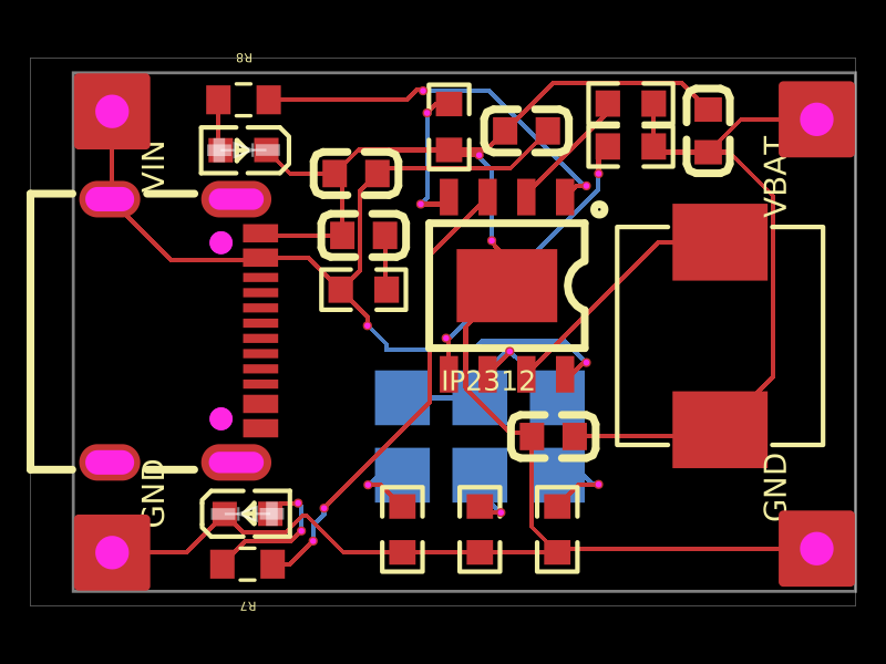 More from this authorkrishnax12/ip2312-fast-charging-moduleThis design implements a compact PCB with a USB-C input port, IP2312 battery charger IC, associated passive components (capacitors, resistors, inductor), output terminals for BAT and GND, and status indicator LEDs, facilitating fast lithium battery charging.
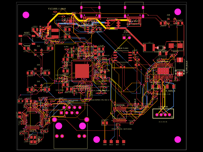 Similar packageshibosoftwaredev/f1c100s-linux-nema8-stepper-controllerRestores component part numbers and CAD models, removes test-point 3D bodies, and validates that solder paste exists only on top-side SMT pads without altering copper or DRC.
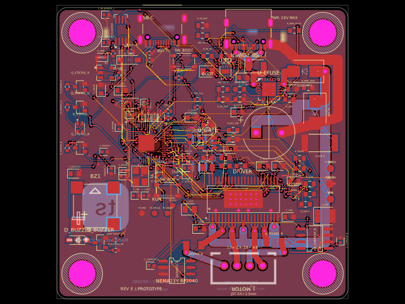 Discover something newimrishabh18/nema-23-stepper-controllerA 57 mm four-layer RP2040 NEMA23 stepper-controller PCB with USB‑C/USB‑PD power input, protected motor rail, DRV8452 dual-winding driver, bidirectional current sensing, temperature/enable interlock, optional magnetic encoder, RGB LED and buzzer status indicators, and motor/test connectors.