krishnax12/t113-minimal-linux
Allwinner T113-S3 dual-Cortex-A7 SoC with integrated 128MB DDR3, multi-rail decoupling, 24MHz and 32.768kHz oscillators, filtering, and exposed test points.
- Version
- 0.1.1
- License
- unset
- Stars
- 0
circuits/Power.tsx
import { TLV62569PDDCR } from "../imports/TLV62569PDDCR"
import { TPS7A2018PDBVR } from "../imports/TPS7A2018PDBVR"
import { TPS3808G18DBVR } from "../imports/TPS3808G18DBVR"
import { TPS3808G33DBVR } from "../imports/TPS3808G33DBVR"
import { TPS3808G01DBVR } from "../imports/TPS3808G01DBVR"

// Allwinner T113-S3 datasheet v1.6 §5.12.1: RTC first, IO >=2 ms
// before CORE/SYS, RESET held >=64 ms after supplies settle.
// Fixed TPS3808 delays: 20 ms nominal / 12 ms minimum; final reset
// 300 ms nominal / 180 ms minimum. These are hardware delays.
// Public nets: V5, GND, VRTC1V8, V3V3, V0V9, V1V5,
// RESET_N and RESET_REQUEST_N (active-low pushbutton input).

const supervisorPins = {
  leftSide: { pins: [6, 5, 3], direction: "top-to-bottom" as const },
  rightSide: { pins: [1, 4, 2], direction: "top-to-bottom" as const },
}

const buckPins = {
  leftSide: { pins: [4, 1, 2], direction: "top-to-bottom" as const },
  rightSide: { pins: [3, 6, 5], direction: "top-to-bottom" as const },
}

// Würth 74437324022 recommended land pattern, datasheet rev003:
// two 1.5 x 2.4 mm pads, 5.2 mm outside span. 2.2uH, 4.05A rated,
// 4.45A typical saturation at 10% drop. No copper beneath body.
const powerInductorFootprint = (
  <footprint>
    <smtpad
      portHints={["pin1"]}
      pcbX={-1.85}
      pcbY={0}
      width={1.5}
      height={2.4}
      shape="rect"
    />
    <smtpad
      portHints={["pin2"]}
      pcbX={1.85}
      pcbY={0}
      width={1.5}
      height={2.4}
      shape="rect"
    />
    <silkscreenpath
      route={[
        { x: -2.2, y: 1.55 },
        { x: -2.2, y: 2.15 },
        { x: 2.2, y: 2.15 },
        { x: 2.2, y: 1.55 },
      ]}
    />
    <silkscreenpath
      route={[
        { x: -2.2, y: -1.55 },
        { x: -2.2, y: -2.15 },
        { x: 2.2, y: -2.15 },
        { x: 2.2, y: -1.55 },
      ]}
    />
    <courtyardrect width={5.7} height={4.9} />
  </footprint>
)

export function Buck({
  id,
  py,
  upper,
  out,
  enable,
  link,
}: {
  id: number
  py: number
  upper: string
  out: string
  enable: string
  link?: number
}) {
  const raw = link ? `${out}_BUCK` : out
  const r = 101 + (id - 101) * 2
  const c = 101 + (id - 101) * 2
  const fb = `FB${id}`
  const sw = `SW${id}`
  return (
    <>
      {link && <net name={raw} />}
      <net name={fb} />
      <net name={sw} />
      <TLV62569PDDCR
        name={`U${id}`}
        pcbX={-44}
        pcbY={py}
        schWidth={3}
        schHeight={3}
        schPinArrangement={buckPins}
        connections={{
          VIN: "net.V5",
          EN: `net.${enable}`,
          GND: "net.GND",
          SW: `net.${sw}`,
          FB: `net.${fb}`,
          PG: "net.RESET_REQUEST_N",
        }}
      />
      <inductor
        name={`L${id}`}
        inductance="2.2uH"
        manufacturerPartNumber="74437324022"
        footprint={powerInductorFootprint}
        pcbX={-38.5}
        pcbY={py - 2.7}
        connections={{ pin1: `net.${sw}`, pin2: `net.${raw}` }}
      />
      <capacitor
        name={`C${c}`}
        capacitance="10uF"
        maxVoltageRating="16V"
        footprint="0805"
        pcbX={-41.5}
        pcbY={py + 4.5}
        pcbRotation={90}
        schRotation={270}
        connections={{ pin1: "net.V5", pin2: "net.GND" }}
      />
      <capacitor
        name={`C${c + 1}`}
        capacitance="22uF"
        maxVoltageRating="16V"
        footprint="1206"
        pcbX={-33.5}
        pcbY={py - 2.5}
        pcbRotation={90}
        schRotation={270}
        connections={{ pin1: `net.${raw}`, pin2: "net.GND" }}
      />
      <group
        name={`feedback_divider_${id}`}
        pcbX={0}
        pcbY={0}
        schLayout={{ layoutMode: "relative" }}
      >
        <resistor
          schX={0}
          schY={1}
          name={`R${r}`}
          resistance={upper}
          tolerance="0.1%"
          footprint="0603"
          pcbX={-48}
          pcbY={py + 2}
          pcbRotation={90}
          schRotation={270}
          connections={{ pin1: `net.${raw}`, pin2: `net.${fb}` }}
        />
        <resistor
          schX={0}
          schY={-1}
          name={`R${r + 1}`}
          resistance="100k"
          tolerance="0.1%"
          footprint="0603"
          pcbX={-48}
          pcbY={py - 1}
          pcbRotation={90}
          schRotation={270}
          connections={{ pin1: `net.${fb}`, pin2: "net.GND" }}
        />
      </group>
      {link && (
        <resistor
          name={`R${link}`}
          resistance="0"
          footprint="1206"
          pcbX={-34}
          pcbY={py + 3}
          connections={{ pin1: `net.${raw}`, pin2: `net.${out}` }}
        />
      )}
    </>
  )
}

export default function Power() {
  return (
    <>
      <net name="EN_IO" />
      <net name="EN_CORE_DDR" />
      <net name="CORE_SENSE" />
      <net name="RESET_REQUEST_N" />
      <net name="RESET_DELAY" />

      {/* First rail is dedicated to the RTC and reset pullup. No battery. */}
      <TPS7A2018PDBVR
        name="U104"
        pcbX={-44}
        pcbY={19}
        schWidth={3}
        schHeight={3}
        schPinArrangement={{
          leftSide: { pins: [1, 3], direction: "top-to-bottom" },
          rightSide: { pins: [5, 4, 2], direction: "top-to-bottom" },
        }}
        connections={{
          IN: "net.V5",
          EN: "net.V5",
          GND: "net.GND",
          OUT: "net.VRTC1V8",
        }}
      />
      <capacitor
        name="C107"
        capacitance="2.2uF"
        maxVoltageRating="16V"
        footprint="0805"
        pcbX={-48}
        pcbY={18}
        schRotation={270}
        connections={{ pin1: "net.V5", pin2: "net.GND" }}
      />
      <capacitor
        name="C108"
        capacitance="2.2uF"
        maxVoltageRating="10V"
        footprint="0805"
        pcbX={-40}
        pcbY={20}
        schRotation={270}
        connections={{ pin1: "net.VRTC1V8", pin2: "net.GND" }}
      />

      {/* U105 waits for RTC >1.67V plus at least12ms; CT intentionally open. */}
      <TPS3808G18DBVR
        name="U105"
        pcbX={-27}
        pcbY={18}
        schWidth={3}
        schHeight={3}
        schPinArrangement={supervisorPins}
        connections={{
          pin6: "net.V5",
          pin5: "net.VRTC1V8",
          pin3: "net.V5",
          pin2: "net.GND",
          pin1: "net.EN_IO",
        }}
      />
      <capacitor
        name="C109"
        capacitance="100nF"
        maxVoltageRating="16V"
        footprint="0603"
        pcbX={-31}
        pcbY={20}
        schRotation={270}
        connections={{ pin1: "net.V5", pin2: "net.GND" }}
      />
      <resistor
        name="R109"
        resistance="10k"
        footprint="0603"
        pcbX={-24}
        pcbY={21.3}
        schRotation={270}
        connections={{ pin1: "net.V5", pin2: "net.EN_IO" }}
      />

      {/* U106 senses the load-side IO rail, including removableR107. */}
      <TPS3808G33DBVR
        name="U106"
        pcbX={-27}
        pcbY={4}
        schWidth={3}
        schHeight={3}
        schPinArrangement={supervisorPins}
        connections={{
          pin6: "net.V5",
          pin5: "net.V3V3",
          pin3: "net.V5",
          pin2: "net.GND",
          pin1: "net.EN_CORE_DDR",
        }}
      />
      <capacitor
        name="C110"
        capacitance="100nF"
        maxVoltageRating="16V"
        footprint="0603"
        pcbX={-30.5}
        pcbY={-0.5}
        schRotation={270}
        connections={{ pin1: "net.V5", pin2: "net.GND" }}
      />
      <resistor
        name="R110"
        resistance="10k"
        footprint="0603"
        pcbX={-24}
        pcbY={7.3}
        schRotation={270}
        connections={{ pin1: "net.V5", pin2: "net.EN_CORE_DDR" }}
      />

      {/* PG outputs of allthree bucks hold /MR low until theiroutputs settle.
        Core threshold0.8181V; hysteresis+threshold+resistortolerance leaves
        margin for the0.8994V regulator's -2% reference limit.
        100k from CT to VDD selects300ms nominal(minimum180ms). */}
      <TPS3808G01DBVR
        name="U107"
        pcbX={-27}
        pcbY={-14}
        schWidth={3}
        schHeight={3}
        schPinArrangement={supervisorPins}
        connections={{
          pin6: "net.V3V3",
          pin5: "net.CORE_SENSE",
          pin3: "net.RESET_REQUEST_N",
          pin2: "net.GND",
          pin1: "net.RESET_N",
          pin4: "net.RESET_DELAY",
        }}
      />
      <resistor
        name="R111"
        resistance="102k"
        tolerance="0.1%"
        footprint="0603"
        pcbX={-30.5}
        pcbY={-13}
        pcbRotation={90}
        schRotation={270}
        connections={{ pin1: "net.V0V9", pin2: "net.CORE_SENSE" }}
      />
      <resistor
        name="R112"
        resistance="100k"
        tolerance="0.1%"
        footprint="0603"
        pcbX={-30.5}
        pcbY={-16}
        pcbRotation={90}
        schRotation={270}
        connections={{ pin1: "net.CORE_SENSE", pin2: "net.GND" }}
      />
      <capacitor
        name="C111"
        capacitance="1nF"
        maxVoltageRating="16V"
        footprint="0603"
        pcbX={-30.5}
        pcbY={-19}
        pcbRotation={90}
        schRotation={270}
        connections={{ pin1: "net.CORE_SENSE", pin2: "net.GND" }}
      />
      <capacitor
        name="C112"
        capacitance="100nF"
        maxVoltageRating="16V"
        footprint="0603"
        pcbX={-26.5}
        pcbY={-18}
        schRotation={270}
        connections={{ pin1: "net.V3V3", pin2: "net.GND" }}
      />
      <resistor
        name="R113"
        resistance="100k"
        footprint="0603"
        pcbX={-24}
        pcbY={-21}
        schRotation={270}
        connections={{ pin1: "net.V3V3", pin2: "net.RESET_DELAY" }}
      />
      <resistor
        name="R114"
        resistance="10k"
        footprint="0603"
        pcbX={-24}
        pcbY={-10}
        schRotation={270}
        connections={{ pin1: "net.VRTC1V8", pin2: "net.RESET_N" }}
      />
      <resistor
        name="R115"
        resistance="10k"
        footprint="0603"
        pcbX={-27}
        pcbY={-10}
        schRotation={270}
        connections={{ pin1: "net.V3V3", pin2: "net.RESET_REQUEST_N" }}
      />
    </>
  )
}
Related Packages
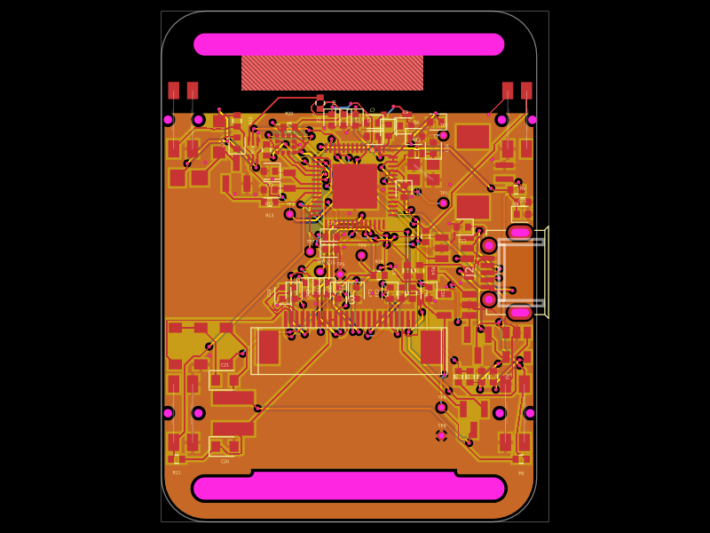 More from this authorkrishnax12/watchy-eink-smartwatchUnfinished prototype (not production-ready): 4 native DRC errors, 2 display-flex intersections, and missing antenna radiator copper remain
 Similar packageliammcg/BayFinder_V1_REVC_ESP32_CARRIERThis design implements a control PCB assembly featuring multiple headers (J1–J4) for ESP32-S3 module connection, integrated USB Type-B and A connectors (J5, J6) for power and data, a protected 5V power circuitry with fuses and TVS diode, an onboard SSD1306 OLED display (J8), and mechanical DIN-rail mounting holes, all interconnected with signal traces, ground pours, and test points.
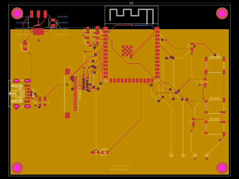 Discover something newShiboSoftwareDev/muse-aipi-lite-replacementA four-layer ESP32-S3 carrier board with USB‑C 5V input, AMS1117 3.3V regulation, FFC display/interface connector, status LED, reset/boot/user buttons, decoupling passives, test points, and ground/power planes.