krishnax12/t113-minimal-linux
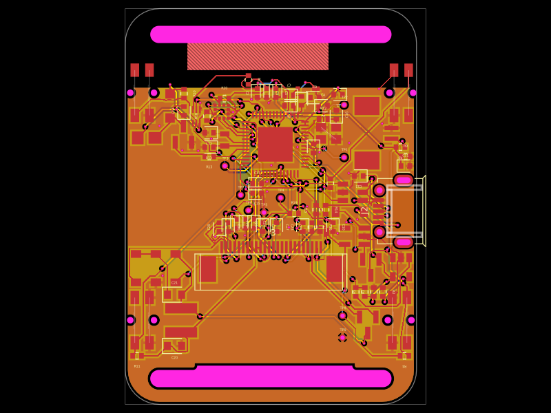
Allwinner T113-S3 dual-Cortex-A7 SoC with integrated 128MB DDR3, multi-rail decoupling, 24MHz and 32.768kHz oscillators, filtering, and exposed test points.
- Version
- 0.1.1
- License
- unset
- Stars
- 0
circuits/Core.tsx
import { T113_S3 } from "../imports/T113_S3"
import { X252024MRB4SI } from "../imports/X252024MRB4SI"
import { Q13FC13500004 } from "../imports/Q13FC13500004"
import { C, R, TP, Wire, Silk } from "./helpers"
import { t113PinLabels } from "./soc-pinmap"
import { Fragment } from "react"

// Source: Allwinner T113-S3 datasheet v1.6 sections4.2,5.3,5.12 and MQ-Dual v1.6.
// External RTC rail rises first. LDOA supplies analog1.8V; LDOB is never tied to DDR.
export const socRails: Record<string, number[]> = {
  GND: [91, 129],
  VRTC1V8: [26],
  V3V3: [29, 34, 66, 77, 83, 128],
  V0V9: [46, 51, 81, 116, 117],
  V1V5: [48, 49],
  LDOA1V8: [20, 28, 50, 65, 89, 97, 107],
}
export const socSpecial: Record<number, string> = {
  7: "SD_D1",
  8: "SD_D0",
  9: "SD_CLK_SOC",
  10: "SD_CMD",
  11: "SD_D3",
  12: "SD_D2",
  13: "SD_CD_N",
  21: "REFCLK24M",
  22: "DXOUT",
  23: "DXIN",
  24: "X32KOUT",
  25: "X32KIN",
  27: "RESET_N",
  30: "LDOB_OUT",
  33: "UART0_RX",
  35: "UART0_TX",
  36: "JTAG_TCK",
  37: "JTAG_TDO",
  38: "JTAG_TDI",
  39: "JTAG_TMS",
  47: "DDR_ZQ",
  90: "VRA2",
  92: "VRA1",
  100: "HPOUTFB",
  101: "GPADC0",
  102: "TP_X1",
  103: "TP_X2",
  104: "TP_Y1",
  105: "TP_Y2",
  110: "TVIN_VRP",
  111: "TVIN_VRN",
  114: "USB0_DM",
  115: "USB0_DP",
}
type SocPinName = keyof typeof t113PinLabels
const socPinNames = Object.keys(t113PinLabels) as SocPinName[]
const usedSignalPins = new Set([
  7, 8, 9, 10, 11, 12, 13, 14, 15, 16, 17, 18, 21, 22, 23, 24, 25, 27, 30, 33,
  35, 47, 52, 90, 92, 100, 110, 111, 114, 115,
])
const allPowerPins = Object.values(socRails).flat()
export const noConnectPins = socPinNames.filter((pin) => {
  const pinNumber = Number(pin.slice(3))
  return !allPowerPins.includes(pinNumber) && !usedSignalPins.has(pinNumber)
})
export const socConnections = Object.fromEntries(
  socPinNames
    .filter((pin) => !noConnectPins.includes(pin))
    .map((pin) => {
      const pinNumber = Number(pin.slice(3))
      const rail = Object.entries(socRails).find(([, pins]) =>
        pins.includes(pinNumber),
      )?.[0]
      return [pinNumber, rail ?? socSpecial[pinNumber] ?? t113PinLabels[pin][0]]
    }),
)

// Exact positions relative to the imported eLQFP footprint (pin1 lower-left).
// Decouplers follow their associated package edge on the bottom; short vias feed the top pads.
const decouplers: [number, string, number, number, number, "top" | "bottom"][] =
  [
    [20, "LDOA1V8", 1.4, -9.5, 90, "bottom"],
    [26, "VRTC1V8", 4, -9.5, 90, "bottom"],
    [34, "V3V3", 9.5, -5.6, 0, "bottom"],
    [46, "V0V9", 9.5, -1.0, 0, "bottom"],
    [48, "V1V5", 9.5, 0.6, 0, "bottom"],
    [49, "V1V5", 11.5, 1.4, 0, "bottom"],
    [50, "LDOA1V8", 9.5, 2.4, 0, "bottom"],
    [51, "V0V9", 11.5, 3.2, 0, "bottom"],
    [65, "LDOA1V8", 6.2, 9.5, 90, "bottom"],
    [66, "V3V3", 4.8, 9.5, 90, "bottom"],
    [77, "V3V3", 1.4, 9.5, 90, "bottom"],
    [81, "V0V9", -0.2, 9.5, 90, "bottom"],
    [83, "V3V3", -1.8, 9.5, 90, "bottom"],
    [89, "LDOA1V8", -4.4, 9.5, 90, "bottom"],
    [97, "LDOA1V8", -9.5, 6.2, 0, "bottom"],
    [107, "LDOA1V8", -9.5, 2.2, 0, "bottom"],
    [116, "V0V9", -9.5, -1.4, 0, "bottom"],
    [117, "V0V9", -11.5, -2.0, 0, "bottom"],
    [128, "V3V3", -9.5, -6.2, 0, "bottom"],
  ]

export function Core() {
  const visiblePins = socPinNames.filter((pin) => !noConnectPins.includes(pin))
  const leftPins = visiblePins.filter(
    (p) => !/^P[B-G]\d/.test(t113PinLabels[p][0]),
  )
  const rightPins = visiblePins.filter((p) => !leftPins.includes(p))
  return (
    <>
      <T113_S3
        name="U_SOC"
        pcbX={0}
        pcbY={0}
        schWidth={7}
        schHeight={12}
        schPinArrangement={{
          leftSide: { pins: leftPins, direction: "top-to-bottom" },
          rightSide: { pins: rightPins, direction: "top-to-bottom" },
        }}
        noConnect={noConnectPins}
        pinAttributes={
          Object.fromEntries(
            Object.entries(t113PinLabels).map(([p]) => {
              const n = Number(p.slice(3))
              return [
                p,
                n === 91 || n === 129
                  ? { requiresGround: true }
                  : n === 28 || n === 30
                    ? { requiresPower: false, providesPower: true }
                    : allPowerPins.includes(n)
                      ? { requiresPower: true }
                      : {},
              ]
            }),
          ) as NonNullable<Parameters<typeof T113_S3>[0]["pinAttributes"]>
        }
      />
      {/* 5.72mm EPAD: all 25 vias stay inside its copper, tied explicitly to GND.
        Drill/pad=0.3/0.6mm. Fabricator must review filling/tenting and paste windows. */}
      {[-2.4, -1.2, 0, 1.2, 2.4].flatMap((x, i) =>
        [-2.4, -1.2, 0, 1.2, 2.4].map((y, j) => (
          <Fragment key={`${i}_${j}`}>
            <via
              name={`V_EP_${i}_${j}`}
              pcbX={x}
              pcbY={y}
              holeDiameter={0.3}
              outerDiameter={0.6}
              fromLayer="top"
              toLayer="bottom"
              connectsTo="net.GND"
              netIsAssignable={false}
            />
          </Fragment>
        )),
      )}
      {Object.entries(socConnections).map(([pin, net]) => (
        <Wire key={pin} from={`.U_SOC > .pin${pin}`} net={net} />
      ))}
      {decouplers.map(([pin, net, x, y, rotation, layer], i) => (
        <C
          key={pin}
          name={`C_SOC_${pin}`}
          value="100nF"
          a={net}
          x={x}
          y={y}
          rotation={rotation}
          layer={layer}
        />
      ))}
      <C
        name="C_LDO_IN"
        value="2.2uF"
        a="V3V3"
        x={5.7}
        y={-11.5}
        footprint="0603"
      />
      <C
        name="C_LDOA"
        value="2.2uF"
        a="LDOA1V8"
        x={0}
        y={-11.5}
        footprint="0603"
      />
      <C
        name="C_LDOB"
        value="2.2uF"
        a="LDOB_OUT"
        x={8.9}
        y={-11.5}
        footprint="0603"
      />
      <C
        name="C_CORE_BULK"
        value="10uF"
        a="V0V9"
        x={-12}
        y={-5}
        footprint="0805"
      />
      <C
        name="C_DRAM_BULK"
        value="10uF"
        a="V1V5"
        x={13}
        y={0}
        footprint="0805"
      />
      <C name="C_DRAM_1U" value="1uF" a="V1V5" x={13} y={-2} footprint="0603" />
      <C
        name="C_AVCC"
        value="2.2uF"
        a="LDOA1V8"
        x={-3.5}
        y={12}
        footprint="0603"
      />
      <R name="R_ZQ" value="240" a="DDR_ZQ" x={10.8} y={-4.2} />
      <C
        name="C_VRA1"
        value="470nF"
        a="VRA1"
        x={-7.3}
        y={12}
        footprint="0603"
      />
      <C
        name="C_VRA2"
        value="470nF"
        a="VRA2"
        x={-7.3}
        y={15.3}
        footprint="0603"
      />
      <C name="C_HPOUTFB" value="100nF" a="HPOUTFB" x={-11} y={5} />
      <C
        name="C_TVIN_VRP"
        value="1uF"
        a="TVIN_VRP"
        x={-12}
        y={1}
        footprint="0603"
      />
      <C
        name="C_TVIN_VRN"
        value="1uF"
        a="TVIN_VRN"
        x={-15.3}
        y={1}
        footprint="0603"
      />
      {/* X252024MRB4SI:24MHz,18pF,20ppm;22pF is the reference-board starting load. */}
      <X252024MRB4SI
        name="Y24M"
        loadCapacitance="18pF"
        pcbX={2}
        pcbY={-16.5}
        connections={{
          pin1: "net.DXIN",
          pin3: "net.DXOUT",
          pin2: "net.GND",
          pin4: "net.GND",
        }}
      />
      <C name="C_X24_IN" value="22pF" a="DXIN" x={0} y={-19} />
      <C name="C_X24_OUT" value="22pF" a="DXOUT" x={4} y={-19} />
      {/* Epson FC-135,32.768kHz,CL12.5pF,20ppm. MQ-Dual v1.6 reference network.
        This belongs to the 1.8V RTC oscillator domain; do not add probe stubs.
        Final routing must keep both resonators close to their corresponding pins. */}
      <Q13FC13500004
        name="Y32K"
        loadCapacitance="12.5pF"
        pcbX={7.8}
        pcbY={-15.3}
        connections={{ pin1: "net.X32KIN", pin2: "net.X32KOUT" }}
      />
      <C name="C_X32_IN" value="22pF" a="X32KIN" x={4.3} y={-13.8} />
      <C name="C_X32_OUT" value="22pF" a="X32KOUT" x={11.3} y={-15.3} />
      <R
        name="R_X32_BIAS"
        value="680k"
        a="X32KIN"
        b="X32KOUT"
        x={7.8}
        y={-18}
      />
      <TP name="TP_CLK" net="REFCLK24M" x={-5} y={-20} />
      <TP name="TP_LDOA" net="LDOA1V8" x={10} y={-18} />
      <TP name="TP_RESET" net="RESET_N" x={16} y={-18} />

      <schematictext
        text="T113-S3: dual Cortex-A7, 128 MB DDR3"
        schX={0}
        schY={6.9}
        fontSize={0.18}
      />
      <schematictext
        text="0.9 V core / 1.5 V DDR / 3.3 V I/O; unused pins NC"
        schX={0}
        schY={6.6}
        fontSize={0.18}
      />
      <Silk text="T113-S3" x={0} y={5} size={1.5} />
      <Silk text="128 MB DDR3" x={0} y={2.5} size={0.8} />
    </>
  )
}
Related Packages
 More from this authorkrishnax12/watchy-eink-smartwatchUnfinished prototype (not production-ready): 4 native DRC errors, 2 display-flex intersections, and missing antenna radiator copper remain
 Similar packageliammcg/BayFinder_V1_REVC_ESP32_CARRIERThis design implements a control PCB assembly featuring multiple headers (J1–J4) for ESP32-S3 module connection, integrated USB Type-B and A connectors (J5, J6) for power and data, a protected 5V power circuitry with fuses and TVS diode, an onboard SSD1306 OLED display (J8), and mechanical DIN-rail mounting holes, all interconnected with signal traces, ground pours, and test points.
 Discover something newShiboSoftwareDev/muse-aipi-lite-replacementA four-layer ESP32-S3 carrier board with USB‑C 5V input, AMS1117 3.3V regulation, FFC display/interface connector, status LED, reset/boot/user buttons, decoupling passives, test points, and ground/power planes.