hrithik18k/metal-touch-panel
A PCB autorouting wrapper that corrects footprint-trace obstacle dimensions, solves routes with a preloaded trace-graph solver, and reports completed traces or routing errors.
- Version
- 1.0.0
- License
- unset
- Stars
- 0
index.circuit.tsx
PCB

Schematic

import { coilAwareRouter } from "./coil-aware-router.browser.js"
import { Fragment } from "react"
import { LDC1614RGHR } from "./imports/LDC1614RGHR"

// 18 mm square, 12 turns, 0.20 mm trace / 0.20 mm spacing.
// Nominal inductance is an estimate; measure with actual target installed.
function spiral() {
  const p: {x:number,y:number}[] = [{x:-9,y:-10},{x:-9,y:-9}]
  for (let i=0;i<12;i++) {
    const r=9-i*0.4
    p.push({x:r,y:-r},{x:r,y:r},{x:-r,y:r},{x:-r,y:-r+0.4})
  }
  p.push({x:-3.6,y:-4.2},{x:-3.6,y:-3.6})
  return p
}
const coil = spiral()
const last = coil[coil.length-1]
function CoilFootprint({channel}: {channel:number}) {
  return <footprint>
    <smtpad portHints={["pin1"]} pcbX={-9} pcbY={-10} width={0.5} height={0.5} shape="rect" coveredWithSolderMask />
    <platedhole portHints={["pin2"]} pcbX={last.x} pcbY={last.y} holeDiameter={0.3} outerDiameter={0.6} shape="circle" coveredWithSolderMask />
    <pcbtrace layer="top" thickness={0.2} route={coil.map(p=>({...p,route_type:"wire" as const,width:0.2,layer:"top" as const}))} />
  </footprint>
}
const sensors = [
  {x:18,y:-15,cx:7,cy:-7}, {x:18,y:15,cx:7,cy:7},
  {x:-18,y:15,cx:-7,cy:7}, {x:-18,y:-15,cx:-7,cy:-7},
]
export default function MetalTouchPanel() {
  return <board width={72} height={64} layers={2} title="Metal Touch / 4-channel LDC1614" autorouter={{algorithmFn:coilAwareRouter}} minTraceWidth={0.15} minViaHoleDiameter={0.3} minViaPadDiameter={0.6} minViaEdgeToPadEdgeClearance={0.15}>
    <schematicsection name="AFE" displayName="Inductance converter" />
    <schematicsection name="Power" displayName="3.3 V host interface" />
    <schematicsection name="Sensors" displayName="Printed sensing coils / tune on bench" />
    <LDC1614RGHR name="U1" layer="bottom" schHeight={1.8} pcbX={0} pcbY={0} schX={0} schY={0} schSectionName="AFE" />
    <capacitor layer="bottom" schOrientation="vertical" name="C5" capacitance="100nF" footprint="0603" pcbRotation={90} pcbX={-0.25} pcbY={-4.2} schX={-9} schY={-4} schSectionName="Power" />
    <capacitor layer="bottom" schOrientation="vertical" name="C6" capacitance="1uF" footprint="0603" pcbX={4} pcbY={-4} schX={-6} schY={-4} schSectionName="Power" />
    <resistor layer="bottom" schRotation={-90} name="R1" resistance="4.7k" footprint="0603" pcbX={-6} pcbY={1} schX={-9} schY={0} schSectionName="Power" />
    <resistor layer="bottom" schRotation={-90} name="R2" resistance="4.7k" footprint="0603" pcbX={-6} pcbY={-2} schX={-6} schY={0} schSectionName="Power" />
    <pinheader layer="bottom" name="J1" pinCount={5} pitch="2.54mm" pcbX={0} pcbY={-28} schX={-12} schY={-2} schSectionName="Power" />
    {sensors.map((s,i)=><Fragment key={i}>
      <inductor name={`L${i+1}`} inductance="3uH" doNotPlace footprint={<CoilFootprint channel={i}/>} pcbX={s.x} pcbY={s.y} schX={9+(i%2)*5} schY={4-Math.floor(i/2)*8} schSectionName="Sensors" />
      <capacitor layer="bottom" schOrientation="vertical" name={`C${i+1}`} pcbRotation={i===1?180:0} capacitance="1nF" footprint="0603" pcbX={s.cx} pcbY={s.cy} schX={9+(i%2)*5} schY={1-Math.floor(i/2)*8} schSectionName="Sensors" />
      <trace from={`U1.IN${i}A`} to={`L${i+1}.pin1`} />
      <trace from={`U1.IN${i}B`} to={`L${i+1}.pin2`} />
      <trace from={`C${i+1}.pin1`} to={`L${i+1}.pin1`} />
      <trace from={`C${i+1}.pin2`} to={`L${i+1}.pin2`} />
      <silkscreentext text={`KEY ${i+1}`} pcbX={s.x} pcbY={s.y} fontSize={1.3}/>
    </Fragment>)}
    {["U1.GND","U1.EP","U1.CLKIN","U1.ADDR","U1.SD","C5.pin2","C6.pin2","J1.pin2"].map(p=><trace key={p} from={p} to="net.GND"/>)}
    {["U1.VDD","C5.pin1","C6.pin1","R1.pin1","R2.pin1","J1.pin1"].map(p=><trace key={p} from={p} to="net.V3V3"/>)}
    <trace from="U1.SCL" to="J1.pin4"/><trace from="U1.SDA" to="J1.pin3"/>
    <trace from="R1.pin2" to="U1.SCL"/><trace from="R2.pin2" to="U1.SDA"/>
    <trace from="U1.INTB" to="J1.pin5"/>
    {[-32,32].flatMap(x=>[-28,28].map(y=><Fragment key={`${x},${y}`}><hole diameter={3.2} pcbX={x} pcbY={y}/></Fragment>))}
    <silkscreentext text="METAL TOUCH  /  REV A" pcbX={0} pcbY={29} fontSize={1.2}/>
    {["3V3","GND","SDA","SCL","INT"].map((label,i)=><Fragment key={label}><silkscreentext text={label} pcbX={5.08-i*2.54} pcbY={-30} fontSize={0.65}/></Fragment>)}
  </board>
}
Related Packages
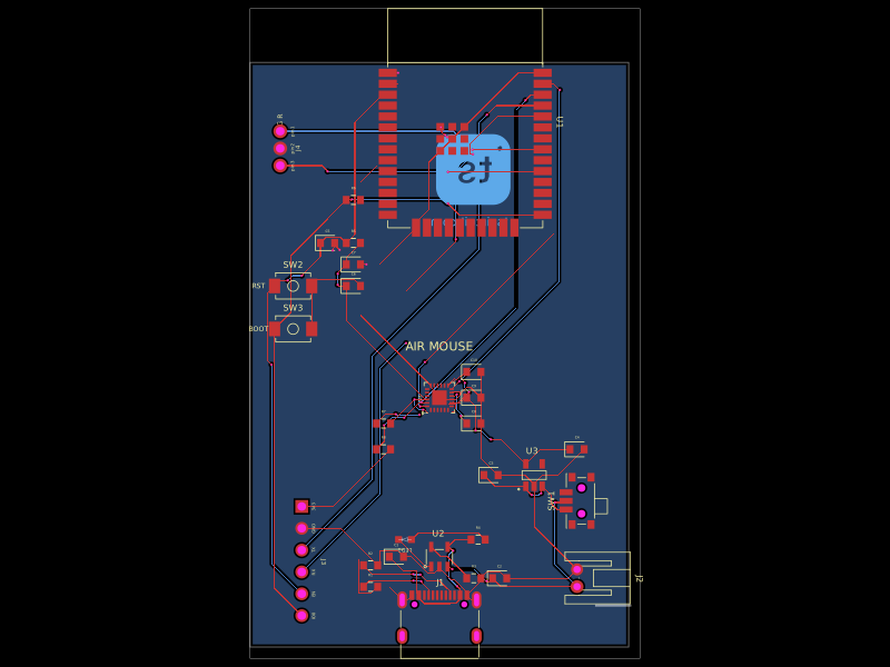 More from this authorhrithik18k/air-mouseA hardware component library defining footprints and 3D models for an ESP32 module, motion sensors, battery chargers, voltage regulator, connectors, switches, and status LED.
 Similar package0hmX/mt41k512m8da-107-it-p-fanoutThis code defines the physical footprint, routing, and layout configuration for a DDR3 memory module using surface-mount pads, vias, and copper traces on a printed circuit board (PCB).
 Discover something newtscircuit/standard-jst-programmer26 × 42 mm USB-C RP2040 programmer with JST and TC2030 IDC SWD, NRST, selectable sensed 5 V / 3.3 V power, RGB status, and importable JST SH/Tag-Connect targets. Top-side assembly.