gokul/cm4-media-carrier
A tscircuit package created by gokul.
- Version
- 0.1.0
- License
- unset
- Stars
- 0
manufacturing/FABRICATION.md
PCB

Schematic

# Fabrication and assembly specification — v0.1.0

## Bare PCB

| Parameter | Requirement |
|---|---|
| Outline | 70.00 × 76.00 mm; route Edge_Cuts centreline |
| Layer order | F_Cu (signals), In1_Cu (GND), In2_Cu (+5 V), B_Cu (low-speed signals) |
| Stackup | JLC04161H-3313, nominal 1.6 mm; listed finished 1.56 mm ±10% |
| Copper | Outer 1 oz / 35 µm; inner 0.5 oz / 15.2 µm |
| L1–L2 / L3–L4 dielectric | 3313 prepreg, 0.0994 mm each |
| Core | 1.265 mm FR-4; use fabricator's specified material dielectric values |
| Finish | ENIG |
| Mask / legend | Green solder mask, white top legend; tent the small vias |
| Minimum routed trace | 0.10 mm |
| Via drill / land | 0.20 / 0.45 mm, through all layers |
| Plane edge setback | 0.50 mm |
| Mounting holes | Four 2.70 mm NPTH at x ±16.5, y −16 and +32 mm |
| Connector guide holes | Two 0.60 mm NPTH; separate NPTH drill file |
| Slots | G85 plated slots in drill-L1-L4.drl; do not turn them into round holes |

All coordinates are millimetres, origin at board centre, +X right, +Y up viewed from top. Nominal board bounds are x ±35 and y ±38. Drills are decimal metric. Copper, drill and outline files share this origin. Do not scale, mirror, or independently recenter layers. Gerber polarity commands and clear regions must be honoured.

The controlled-impedance geometry is based on the named fabricator stackup calculator. Order impedance control and have the fabricator use these targets; do not substitute a generic 1.6 mm stackup without recalculating the traces:

| Signals | Layer/reference | Differential target | Finished trace width | Pair edge gap |
|---|---|---|---|---|
| HDMI0 D2/D1/D0/CLK | L1 / solid L2 GND | 100 Ω ±10% | 0.1041 mm | 0.1501 mm |
| USB programming D+/D− | L1 / solid L2 GND | 90 Ω ±10% | 0.1356 mm | 0.1501 mm |

Use edge-coupled microstrip, not coplanar geometry. The specified targets apply to the coupled sections; connector fanouts are short discontinuities. Fabricator etch compensation is allowed to achieve finished dimensions and impedance. Require routine electrical test and DFM; unresolved manufacturing exceptions must be corrected before ordering. This is the normal factory acceptance step, not a claim that a board house has already reviewed this order.

## Assembly

All 19 carrier components mount on top. Use the exact MPNs in BOM.csv. Fit two DF40C-100DS-0.4V(51) sockets; the 3 mm-stack alternative changes the assembly height and is not a drop-in mechanical substitution for this release.

Use a 0.10 mm top stencil as the starting process specification. The socket openings are 0.70 × 0.20 mm, giving a nominal aperture area ratio of 0.778 at this thickness. There is no bottom stencil. Reflow the SMT joints using the component manufacturers' profiles; hand/selectively solder the connector stakes and the two service headers afterward. The overlapping Micro-B shell land apertures form one continuous stencil opening where they overlap. Have the assembler merge coincident stencil geometry, not print extra paste passes. Fit the CM4 only after reflow and cleaning.

PLACEMENT.csv includes every component's design origin, rotation and an explicit physical pin-1 coordinate. This makes polarity review possible without guessing feeder rotation. For J_USB, internal library pin 1 is shield tab EH2; use the A/B contact aliases in the source for its USB contacts. Both LEDs have **pin 1 = cathode, on the right**, aligned to their adjacent vertical silkscreen bar. AP2331 pin 1 is GND. Pin 1 of both CM4 sockets is the upper-left pad in the top view.

USB and HDMI mouths extend to or beyond the corresponding board edge. Keep external cable access clear; enclosure wall and plug-overmould dimensions are not defined by this bare-PCB release. Use nonconductive M2.5 mounting hardware, 1.5 mm board-to-board spacing, and avoid loading the CM4 sockets with fastener torque. The metal-screw-head clearance has not been qualified.

## First-article verification

Inspect socket pin alignment, solder bridges, LED polarity and plated slots under magnification. Before fitting the CM4, check 5 V-to-GND for a short and verify the HDMI power-switch pinout. With a current-limited 5 V source, verify input voltage and the power LED; then remove power and install the CM4.

Record first boot/current draw, minimum voltage at the CM4 under CPU/Wi-Fi/display load, eMMC programming, reset/boot jumper operation, activity LED, HDMI video/audio/CEC, external-antenna operation and thermal behaviour. Start with a small prototype lot. These physical acceptance tests have not been performed on this design.
Related Packages
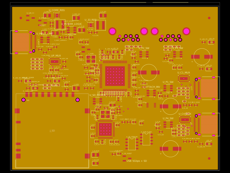 More from this authorgokul/usb3-sd-hubEngineering draft: four-layer, computer-powered USB 3 hub with one USB-C host socket, two USB-C and two USB-A accessory sockets, and a full-size SD slot. Board and three schematic previews are available. Routing and production checks are incomplete; not fabrication ready.
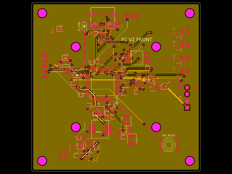 Discover something newmohan-bee/flight-controller-v2A 64 mm STM32F405 flight-controller PCB with ICM-42688 IMU, SPI flash, USB-C/ESD, battery buck and 3.3 V regulation, four motor outputs, service I/O, and PETG standoff mounting hardware.