gokul/cm4-media-carrier
A tscircuit package created by gokul.
- Version
- 0.1.0
- License
- unset
- Stars
- 0
index.tsx
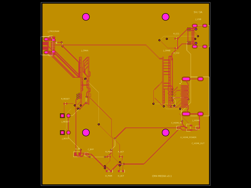
PCB
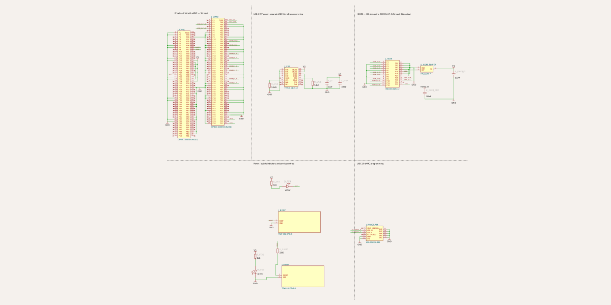
Schematic
import { routeOuterLayers } from "./routing"
import { PowerConnections } from "./power-connections"
import { highSpeedTracePaths } from "./high-speed-paths"
import { SocketA } from "./components/SocketA"
import { SocketB } from "./components/SocketB"
import { Usb as UsbProgramming } from "./components/Usb"
import { Hdmi } from "./components/Hdmi"
import { TYPE_C_31_M_12 as UsbC } from "./imports/TYPE_C_31_M_12"
import { AP2331W_7 } from "./imports/AP2331W_7"
import { groundPins } from "./components/cm4-pins"
import { KingbrightLed } from "./components/KingbrightLed"

const hdmiPairs = [
  { name: "HDMI_D2", positive: 170, negative: 172, hdmiPositive: 1, hdmiNegative: 3 },
  { name: "HDMI_D1", positive: 176, negative: 178, hdmiPositive: 4, hdmiNegative: 6 },
  { name: "HDMI_D0", positive: 182, negative: 184, hdmiPositive: 7, hdmiNegative: 9 },
  { name: "HDMI_CLK", positive: 188, negative: 190, hdmiPositive: 10, hdmiNegative: 12 },
]
const moduleConnections = {
  ...Object.fromEntries(groundPins.map(pin => [`pin${pin}`, "net.GND"])),
  ...Object.fromEntries([77,79,81,83,85,87].map(pin => [`pin${pin}`, "net.V5"])),
  pin78: "net.V3", pin84: "net.V3", pin86: "net.V3",
  pin21: "net.ACT", pin92: "net.RUN", pin93: "net.BOOT",
  pin151: "net.CEC", pin153: "net.HPD", pin199: "net.DDC_SDA", pin200: "net.DDC_SCL",
}

const usedModulePins = new Set([
  ...Object.keys(moduleConnections).map(pin => Number(pin.slice(3))),
  ...hdmiPairs.flatMap(pair => [pair.positive, pair.negative]), 103, 105,
])
const unusedSocketPins = (offset: number) => Array.from({length: 100}, (_, i) => i + 1)
  .filter(pin => !usedModulePins.has(pin + offset)).map(pin => `pin${pin}`)

export default () => (
  <board pcbRelative width="70mm" height="76mm" layers={4} thickness="1.6mm"
    title="CM4 media carrier — engineering prototype"
    autorouter="auto_local" minTraceWidth="0.1mm" minViaHoleDiameter="0.2mm" minViaPadDiameter="0.45mm" schAutoLayoutEnabled pcbStyle={{silkscreenFontSize:0.8}}
    schLayout={{ flexDirection: "column", gap: 5 }}>
    <autoroutingphase name="MATCHED_HIGH_SPEED" phaseIndex={0} connections={highSpeedTracePaths.map(path => path.connection)} pcbTracePaths={highSpeedTracePaths} />
    <autoroutingphase name="POWER_AND_CONTROL" autorouter={{local:true,algorithmFn:routeOuterLayers}} />

    <silkscreentext text="J_CM4A" pcbX={-16.96} pcbY={18} fontSize="0.8mm" />
    <silkscreentext text="J_CM4B" pcbX={16.96} pcbY={18} fontSize="0.8mm" />
    <silkscreentext text="J_USB" pcbX={30} pcbY={31} fontSize="0.8mm" />
    <silkscreentext text="J_HDMI" pcbX={29} pcbY={-11} fontSize="0.8mm" />
    <silkscreentext text="J_PROGRAM" pcbX={-30} pcbY={26} fontSize="0.8mm" />
    <silkscreentext text="R_CC1" pcbX={21} pcbY={25} fontSize="0.8mm" />
    <silkscreentext text="R_CC2" pcbX={21} pcbY={17} fontSize="0.8mm" />
    <silkscreentext text="C_IN" pcbX={-20} pcbY={-22.8} fontSize="0.8mm" />
    <silkscreentext text="C_BYP" pcbX={-14.5} pcbY={-23} fontSize="0.8mm" />
    <silkscreentext text="U_HDMI_POWER" pcbX={26} pcbY={-18} fontSize="0.8mm" />
    <silkscreentext text="C_HDMI_IN" pcbX={21} pcbY={-12} fontSize="0.8mm" />
    <silkscreentext text="C_HDMI_OUT" pcbX={30} pcbY={-20.5} fontSize="0.8mm" />
    <silkscreentext text="R_PWR" pcbX={-7} pcbY={-24} fontSize="0.8mm" />
    <silkscreentext text="R_ACT" pcbX={-2} pcbY={-24} fontSize="0.8mm" />
    <silkscreentext text="D_PWR" pcbX={-7} pcbY={-34} fontSize="0.8mm" />
    <silkscreentext text="D_ACT" pcbX={-2} pcbY={-34} fontSize="0.8mm" />
    <silkscreentext text="J_BOOT" pcbX={-25} pcbY={-18.5} fontSize="0.8mm" />
    <silkscreentext text="J_RESET" pcbX={-25} pcbY={-11.5} fontSize="0.8mm" />
    <silkscreentext text="R_RESET" pcbX={-25} pcbY={-2} fontSize="0.8mm" />
    <silkscreentext text="5V / 3A" pcbX={30} pcbY={34} fontSize="1mm" />
    <silkscreentext text="CM4 MEDIA v0.1" pcbX={15} pcbY={-34} fontSize="1mm" />
    <PowerConnections />
    <net name="GND" isGroundNet /><net name="V5" isPowerNet nominalTraceWidth="0.3mm" /><net name="V3" isPowerNet /><net name="HDMI_5V" isPowerNet />
    <copperpour name="GROUND_REFERENCE" layer="inner1" connectsTo="net.GND" unbroken clearance="0.2mm" boardEdgeMargin="0.5mm" useThermalReliefs={false} />
    <copperpour name="POWER_PLANE" layer="inner2" connectsTo="net.V5" unbroken clearance="0.2mm" boardEdgeMargin="0.5mm" useThermalReliefs={false} />
    <schematicsection name="COMPUTE" displayName="Wireless CM4 with eMMC — 5V input" />
      <SocketA pcbStyle={{silkscreenTextVisibility:"hidden"}} schSectionName="COMPUTE" name="J_CM4A" noConnect={unusedSocketPins(0)} pcbX={-16.96} pcbY={5.5}
        connections={Object.fromEntries(Object.entries(moduleConnections).filter(([pin]) => Number(pin.slice(3)) <= 100))} />
      <SocketB pcbStyle={{silkscreenTextVisibility:"hidden"}} schSectionName="COMPUTE" name="J_CM4B" noConnect={unusedSocketPins(100)} pcbX={16.96} pcbY={5.5}
        connections={Object.fromEntries(Object.entries(moduleConnections).filter(([pin]) => Number(pin.slice(3)) > 100).map(([pin, net]) => [`pin${Number(pin.slice(3)) - 100}`, net]))} />
      {[-16.5,16.5].flatMap(x => [-16,32].map(y => <group key={`${x}:${y}`} pcbRelative><hole pcbX={x} pcbY={y} diameter="2.7mm" /></group>))}


    <schematicsection name="POWER" displayName="USB-C 5V power; separate USB Micro-B programming" />
      <UsbC pcbStyle={{silkscreenTextVisibility:"hidden"}} schSectionName="POWER" name="J_USB" allowOffBoard noConnect={["SBU1","SBU2","DP1","DP2","DN1","DN2"]} pcbPositionMode="relative_to_board_anchor" pcbX={30} pcbY={24} pcbRotation={90} connections={{
        VBUS1:"net.V5", VBUS2:"net.V5", GND1:"net.GND", GND2:"net.GND",
        EH1:"net.GND",EH2:"net.GND",EH3:"net.GND",EH4:"net.GND",
        CC1:".R_CC1 > .pin1", CC2:".R_CC2 > .pin1",

      }} />
      <resistor pcbStyle={{silkscreenTextVisibility:"hidden"}} schSectionName="POWER" name="R_CC1" resistance="5.1k" manufacturerPartNumber="RC0402FR-075K1L" footprint="0402" pcbPositionMode="relative_to_board_anchor" pcbX={21} pcbY={23} connections={{pin2:"net.GND"}} />
      <resistor pcbStyle={{silkscreenTextVisibility:"hidden"}} schSectionName="POWER" name="R_CC2" resistance="5.1k" manufacturerPartNumber="RC0402FR-075K1L" footprint="0402" pcbPositionMode="relative_to_board_anchor" pcbX={21} pcbY={19} connections={{pin2:"net.GND"}} />
      <capacitor pcbStyle={{silkscreenTextVisibility:"hidden"}} schSectionName="POWER" name="C_IN" manufacturerPartNumber="GRM21BR61A106KE19L" capacitance="10uF" maxVoltageRating="10V" footprint="0805" pcbPositionMode="relative_to_board_anchor" pcbX={-20} pcbY={-25} connections={{pin1:"net.V5",pin2:"net.GND"}} />
      <capacitor pcbStyle={{silkscreenTextVisibility:"hidden"}} schSectionName="POWER" name="C_BYP" manufacturerPartNumber="GRM155R71C104KA88D" capacitance="100nF" maxVoltageRating="16V" footprint="0402" pcbPositionMode="relative_to_board_anchor" pcbX={-16} pcbY={-25} connections={{pin1:"net.V5",pin2:"net.GND"}} />

    <schematicsection name="VIDEO" displayName="HDMI0 — 100 ohm pairs; AP2331: 2.7–5.2V input, 0.2A output" />
      <AP2331W_7 pcbStyle={{silkscreenTextVisibility:"hidden"}} schSectionName="VIDEO" name="U_HDMI_POWER" pcbX={26} pcbY={-14} connections={{IN:"net.V5",OUT:"net.HDMI_5V",GND:"net.GND"}} />
      <capacitor pcbStyle={{silkscreenTextVisibility:"hidden"}} schSectionName="VIDEO" name="C_HDMI_IN" capacitance="100nF" maxVoltageRating="16V" manufacturerPartNumber="GRM155R71C104KA88D" footprint="0402" pcbX={22} pcbY={-14} connections={{pin1:"net.V5",pin2:"net.GND"}} />
      <capacitor pcbStyle={{silkscreenTextVisibility:"hidden"}} schSectionName="VIDEO" name="C_HDMI_OUT" capacitance="100nF" maxVoltageRating="16V" manufacturerPartNumber="GRM155R71C104KA88D" footprint="0402" pcbX={30} pcbY={-14} connections={{pin1:"net.HDMI_5V",pin2:"net.GND"}} />
      <Hdmi pcbStyle={{silkscreenTextVisibility:"hidden"}} schSectionName="VIDEO" name="J_HDMI" noConnect={["pin14"]} manufacturerPartNumber="690-019-298-412" pcbPositionMode="relative_to_board_anchor" pcbX={25} pcbY={-1} pcbRotation={90} pinLabels={Object.fromEntries([...Array.from({length:19},(_,i)=>[`pin${i+1}`,[`P${i+1}`]]),...[1,2,3,4].map(i=>[`SH${i}`,[`SH${i}`]])])}
        connections={{pin2:"net.GND",pin5:"net.GND",pin8:"net.GND",pin11:"net.GND",pin17:"net.GND",
          pin13:"net.CEC",pin15:"net.DDC_SCL",pin16:"net.DDC_SDA",pin18:"net.HDMI_5V",pin19:"net.HPD",
          SH1:"net.GND",SH2:"net.GND",SH3:"net.GND",SH4:"net.GND"}} />

    <schematicsection name="STATUS" displayName="Power / activity indicators and service controls" />
      <resistor pcbStyle={{silkscreenTextVisibility:"hidden"}} schSectionName="STATUS" name="R_PWR" resistance="1k" manufacturerPartNumber="RC0402FR-071KL" footprint="0402" pcbPositionMode="relative_to_board_anchor" pcbX={-7} pcbY={-26} connections={{pin1:"net.V5",pin2:".D_PWR > .anode"}} />
      <KingbrightLed pcbStyle={{silkscreenTextVisibility:"hidden"}} schSectionName="STATUS" name="D_PWR" manufacturerPartNumber="APT1608SGC" color="green" pcbPositionMode="relative_to_board_anchor" pcbX={-7} pcbY={-32} connections={{cathode:"net.GND"}} />
      <resistor pcbStyle={{silkscreenTextVisibility:"hidden"}} schSectionName="STATUS" name="R_ACT" resistance="1k" manufacturerPartNumber="RC0402FR-071KL" footprint="0402" pcbPositionMode="relative_to_board_anchor" pcbX={-2} pcbY={-26} connections={{pin1:"net.V3",pin2:".D_ACT > .anode"}} />
      <KingbrightLed pcbStyle={{silkscreenTextVisibility:"hidden"}} schSectionName="STATUS" name="D_ACT" manufacturerPartNumber="APT1608SYC/J3-AMT" color="yellow" pcbPositionMode="relative_to_board_anchor" pcbX={-2} pcbY={-32} connections={{cathode:"net.ACT"}} />
      <connector pcbStyle={{silkscreenTextVisibility:"hidden"}} schSectionName="STATUS" name="J_BOOT" schRotation={0} schPinArrangement={{leftSide:[1,2]}} schWidth={4} schHeight={2} pinLabels={{pin1:["BOOT"],pin2:["GND"]}} manufacturerPartNumber="TSW-102-07-G-S" footprint="pinrow2" pcbPositionMode="relative_to_board_anchor" pcbX={-25} pcbY={-16} connections={{pin1:"net.BOOT",pin2:"net.GND"}} />
      <connector pcbStyle={{silkscreenTextVisibility:"hidden"}} schSectionName="STATUS" name="J_RESET" schRotation={0} schPinArrangement={{leftSide:[1,2]}} schWidth={4} schHeight={2} pinLabels={{pin1:["RESET"],pin2:["GND"]}} manufacturerPartNumber="TSW-102-07-G-S" footprint="pinrow2" pcbPositionMode="relative_to_board_anchor" pcbX={-25} pcbY={-9} connections={{pin1:".R_RESET > .pin1",pin2:"net.GND"}} />
      <resistor pcbStyle={{silkscreenTextVisibility:"hidden"}} schSectionName="STATUS" name="R_RESET" resistance="220" manufacturerPartNumber="RC0402FR-07220RL" footprint="0402" pcbPositionMode="relative_to_board_anchor" pcbX={-25} pcbY={-4} connections={{pin2:"net.RUN"}} />

    <trace name="V3_MODULE_LINK" from=".J_CM4A > .pin78" to=".J_CM4A > .pin84" thickness="0.1mm" pcbPath={[".J_CM4A > .pin78",{x:2.54,y:-5.4},{x:2.54,y:-6.6},".J_CM4A > .pin84"]} />
    <trace name="V3_REFERENCE_LINK" from=".J_CM4A > .pin84" to=".J_CM4A > .pin86" thickness="0.1mm" pcbStraightLine />
    <bus name="HDMI_TOP_LAYER" connections={hdmiPairs.flatMap(pair => [`${pair.name}_P`, `${pair.name}_N`])} pcbAllowedLayers={["top"]} pcbTraceWidth="0.1041mm" />
    {hdmiPairs.map((pair, pairIndex) => <group pcbRelative pcbX={0} pcbY={0} key={pair.name}>
      <trace name={`${pair.name}_P`} from={`.J_CM4B > .pin${pair.positive - 100}`} to={`.J_HDMI > .pin${pair.hdmiPositive}`} thickness="0.1041mm" />
      <trace name={`${pair.name}_N`} from={`.J_CM4B > .pin${pair.negative - 100}`} to={`.J_HDMI > .pin${pair.hdmiNegative}`} thickness="0.1041mm" />
      <differentialpair name={pair.name} positiveConnection={`${pair.name}_P`} negativeConnection={`${pair.name}_N`} maxLengthSkew="0.15mm" targetDifferentialImpedance="100ohm" pcbTraceGap="0.1501mm" maxUncoupledLength="2mm" />
    </group>)}
    <schematicsection name="PROGRAM" displayName="USB 2.0 eMMC programming" />
    <UsbProgramming pcbStyle={{silkscreenTextVisibility:"hidden"}} schSectionName="PROGRAM" name="J_PROGRAM" allowOffBoard manufacturerPartNumber="690-005-298-486" pcbX={-32.99} pcbY={20} pcbRotation={270}
      pinLabels={{pin1:["VBUS_UNUSED"],pin2:["USB_N"],pin3:["USB_P"],pin4:["ID_UNUSED"],pin5:["GND"],SH1:["SH1"],SH2:["SH2"],SH3:["SH3"],SH4:["SH4"],SH5:["SH5"],SH6:["SH6"]}}
      noConnect={["pin1","pin4"]} connections={{pin5:"net.GND",SH1:"net.GND",SH2:"net.GND",SH3:"net.GND",SH4:"net.GND",SH5:"net.GND",SH6:"net.GND"}} />
    <trace thickness="0.1356mm" name="USB_DATA_P" from=".J_CM4B > .pin5" to=".J_PROGRAM > .pin3" />
    <bus name="USB_TOP_LAYER" connections={["USB_DATA_P","USB_DATA_N"]} pcbAllowedLayers={["top"]} pcbTraceWidth="0.1356mm" />
    <differentialpair name="USB2" positiveConnection="USB_DATA_P" negativeConnection="USB_DATA_N" maxLengthSkew="0.15mm" targetDifferentialImpedance="90ohm" pcbTraceGap="0.1501mm" maxUncoupledLength="2mm" />
    <trace thickness="0.1356mm" name="USB_DATA_N" from=".J_CM4B > .pin3" to=".J_PROGRAM > .pin2" />

  </board>
)
Related Packages
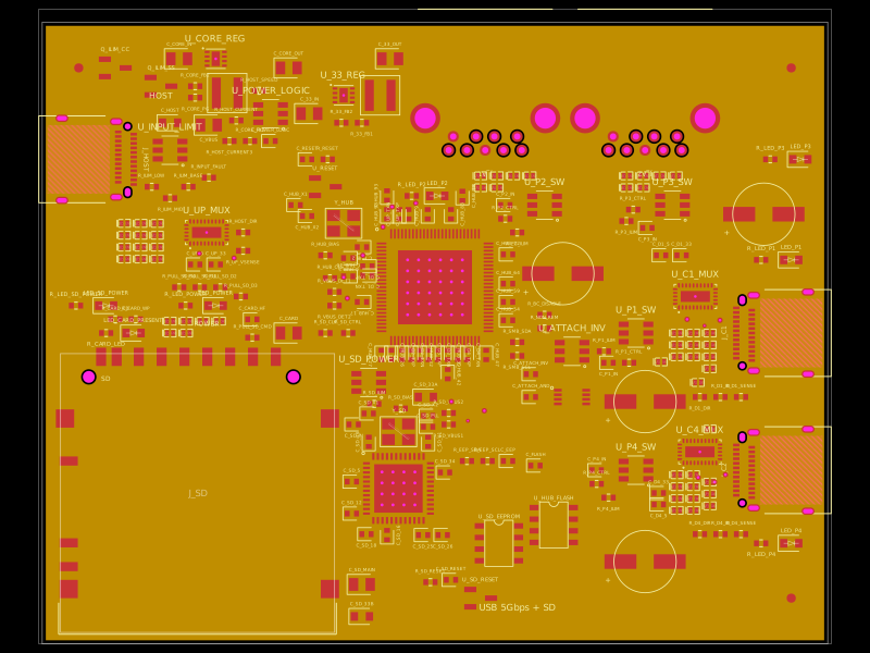 More from this authorgokul/usb3-sd-hubEngineering draft: four-layer, computer-powered USB 3 hub with one USB-C host socket, two USB-C and two USB-A accessory sockets, and a full-size SD slot. Board and three schematic previews are available. Routing and production checks are incomplete; not fabrication ready.
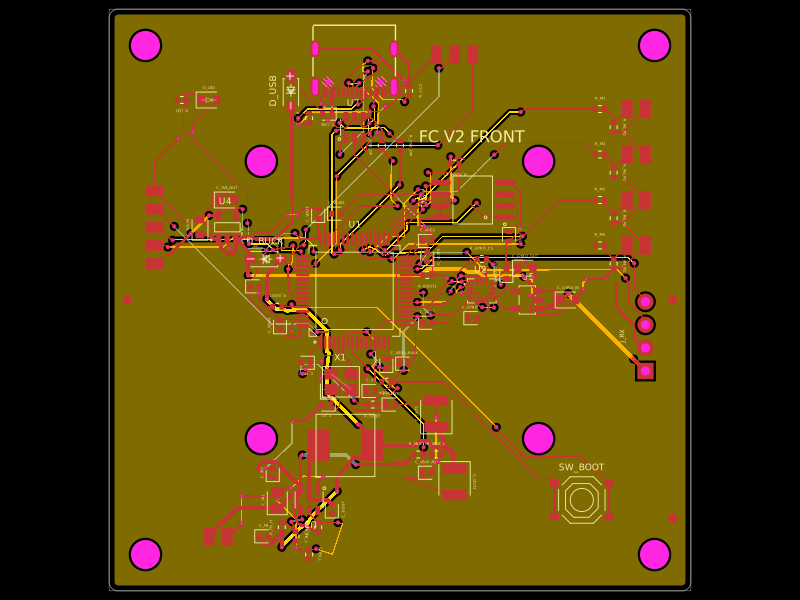 Discover something newmohan-bee/flight-controller-v2A 64 mm STM32F405 flight-controller PCB with ICM-42688 IMU, SPI flash, USB-C/ESD, battery buck and 3.3 V regulation, four motor outputs, service I/O, and PETG standoff mounting hardware.