gokul/cm4-media-carrier
A tscircuit package created by gokul.
- Version
- 0.1.0
- License
- unset
- Stars
- 0
components/SocketA.tsx
import socketModel from "../models/socket.glb"
import { type ChipProps } from "tscircuit"
export const SocketA = (props: ChipProps) => (<connector cadModel={{glbUrl:socketModel,modelUnitToMmScale:1,modelOriginPosition:{x:0,y:0,z:0},modelBounds:{min:{x:-1.69,y:-11.3,z:-0.05},max:{x:1.69,y:11.3,z:1.4}}}} manufacturerPartNumber="DF40C-100DS-0.4V(51)" pinLabels={Object.fromEntries(Array.from({length:100},(_,i)=>[`pin${i+1}`,[`P${i+1}`]]))} pinAttributes={Object.fromEntries(Array.from({length:100},(_,i)=>[`pin${i+1}`,{isPassive:true}]))} footprint={<footprint insertionDirection="from_above">
<smtpad solderPasteMargin={0} portHints={["1"]} pcbX={-1.540} pcbY={9.800} layer="top" width="0.7mm" height="0.2mm" shape="rect" />
<smtpad solderPasteMargin={0} portHints={["2"]} pcbX={1.540} pcbY={9.800} layer="top" width="0.7mm" height="0.2mm" shape="rect" />
<smtpad solderPasteMargin={0} portHints={["3"]} pcbX={-1.540} pcbY={9.400} layer="top" width="0.7mm" height="0.2mm" shape="rect" />
<smtpad solderPasteMargin={0} portHints={["4"]} pcbX={1.540} pcbY={9.400} layer="top" width="0.7mm" height="0.2mm" shape="rect" />
<smtpad solderPasteMargin={0} portHints={["5"]} pcbX={-1.540} pcbY={9.000} layer="top" width="0.7mm" height="0.2mm" shape="rect" />
<smtpad solderPasteMargin={0} portHints={["6"]} pcbX={1.540} pcbY={9.000} layer="top" width="0.7mm" height="0.2mm" shape="rect" />
<smtpad solderPasteMargin={0} portHints={["7"]} pcbX={-1.540} pcbY={8.600} layer="top" width="0.7mm" height="0.2mm" shape="rect" />
<smtpad solderPasteMargin={0} portHints={["8"]} pcbX={1.540} pcbY={8.600} layer="top" width="0.7mm" height="0.2mm" shape="rect" />
<smtpad solderPasteMargin={0} portHints={["9"]} pcbX={-1.540} pcbY={8.200} layer="top" width="0.7mm" height="0.2mm" shape="rect" />
<smtpad solderPasteMargin={0} portHints={["10"]} pcbX={1.540} pcbY={8.200} layer="top" width="0.7mm" height="0.2mm" shape="rect" />
<smtpad solderPasteMargin={0} portHints={["11"]} pcbX={-1.540} pcbY={7.800} layer="top" width="0.7mm" height="0.2mm" shape="rect" />
<smtpad solderPasteMargin={0} portHints={["12"]} pcbX={1.540} pcbY={7.800} layer="top" width="0.7mm" height="0.2mm" shape="rect" />
<smtpad solderPasteMargin={0} portHints={["13"]} pcbX={-1.540} pcbY={7.400} layer="top" width="0.7mm" height="0.2mm" shape="rect" />
<smtpad solderPasteMargin={0} portHints={["14"]} pcbX={1.540} pcbY={7.400} layer="top" width="0.7mm" height="0.2mm" shape="rect" />
<smtpad solderPasteMargin={0} portHints={["15"]} pcbX={-1.540} pcbY={7.000} layer="top" width="0.7mm" height="0.2mm" shape="rect" />
<smtpad solderPasteMargin={0} portHints={["16"]} pcbX={1.540} pcbY={7.000} layer="top" width="0.7mm" height="0.2mm" shape="rect" />
<smtpad solderPasteMargin={0} portHints={["17"]} pcbX={-1.540} pcbY={6.600} layer="top" width="0.7mm" height="0.2mm" shape="rect" />
<smtpad solderPasteMargin={0} portHints={["18"]} pcbX={1.540} pcbY={6.600} layer="top" width="0.7mm" height="0.2mm" shape="rect" />
<smtpad solderPasteMargin={0} portHints={["19"]} pcbX={-1.540} pcbY={6.200} layer="top" width="0.7mm" height="0.2mm" shape="rect" />
<smtpad solderPasteMargin={0} portHints={["20"]} pcbX={1.540} pcbY={6.200} layer="top" width="0.7mm" height="0.2mm" shape="rect" />
<smtpad solderPasteMargin={0} portHints={["21"]} pcbX={-1.540} pcbY={5.800} layer="top" width="0.7mm" height="0.2mm" shape="rect" />
<smtpad solderPasteMargin={0} portHints={["22"]} pcbX={1.540} pcbY={5.800} layer="top" width="0.7mm" height="0.2mm" shape="rect" />
<smtpad solderPasteMargin={0} portHints={["23"]} pcbX={-1.540} pcbY={5.400} layer="top" width="0.7mm" height="0.2mm" shape="rect" />
<smtpad solderPasteMargin={0} portHints={["24"]} pcbX={1.540} pcbY={5.400} layer="top" width="0.7mm" height="0.2mm" shape="rect" />
<smtpad solderPasteMargin={0} portHints={["25"]} pcbX={-1.540} pcbY={5.000} layer="top" width="0.7mm" height="0.2mm" shape="rect" />
<smtpad solderPasteMargin={0} portHints={["26"]} pcbX={1.540} pcbY={5.000} layer="top" width="0.7mm" height="0.2mm" shape="rect" />
<smtpad solderPasteMargin={0} portHints={["27"]} pcbX={-1.540} pcbY={4.600} layer="top" width="0.7mm" height="0.2mm" shape="rect" />
<smtpad solderPasteMargin={0} portHints={["28"]} pcbX={1.540} pcbY={4.600} layer="top" width="0.7mm" height="0.2mm" shape="rect" />
<smtpad solderPasteMargin={0} portHints={["29"]} pcbX={-1.540} pcbY={4.200} layer="top" width="0.7mm" height="0.2mm" shape="rect" />
<smtpad solderPasteMargin={0} portHints={["30"]} pcbX={1.540} pcbY={4.200} layer="top" width="0.7mm" height="0.2mm" shape="rect" />
<smtpad solderPasteMargin={0} portHints={["31"]} pcbX={-1.540} pcbY={3.800} layer="top" width="0.7mm" height="0.2mm" shape="rect" />
<smtpad solderPasteMargin={0} portHints={["32"]} pcbX={1.540} pcbY={3.800} layer="top" width="0.7mm" height="0.2mm" shape="rect" />
<smtpad solderPasteMargin={0} portHints={["33"]} pcbX={-1.540} pcbY={3.400} layer="top" width="0.7mm" height="0.2mm" shape="rect" />
<smtpad solderPasteMargin={0} portHints={["34"]} pcbX={1.540} pcbY={3.400} layer="top" width="0.7mm" height="0.2mm" shape="rect" />
<smtpad solderPasteMargin={0} portHints={["35"]} pcbX={-1.540} pcbY={3.000} layer="top" width="0.7mm" height="0.2mm" shape="rect" />
<smtpad solderPasteMargin={0} portHints={["36"]} pcbX={1.540} pcbY={3.000} layer="top" width="0.7mm" height="0.2mm" shape="rect" />
<smtpad solderPasteMargin={0} portHints={["37"]} pcbX={-1.540} pcbY={2.600} layer="top" width="0.7mm" height="0.2mm" shape="rect" />
<smtpad solderPasteMargin={0} portHints={["38"]} pcbX={1.540} pcbY={2.600} layer="top" width="0.7mm" height="0.2mm" shape="rect" />
<smtpad solderPasteMargin={0} portHints={["39"]} pcbX={-1.540} pcbY={2.200} layer="top" width="0.7mm" height="0.2mm" shape="rect" />
<smtpad solderPasteMargin={0} portHints={["40"]} pcbX={1.540} pcbY={2.200} layer="top" width="0.7mm" height="0.2mm" shape="rect" />
<smtpad solderPasteMargin={0} portHints={["41"]} pcbX={-1.540} pcbY={1.800} layer="top" width="0.7mm" height="0.2mm" shape="rect" />
<smtpad solderPasteMargin={0} portHints={["42"]} pcbX={1.540} pcbY={1.800} layer="top" width="0.7mm" height="0.2mm" shape="rect" />
<smtpad solderPasteMargin={0} portHints={["43"]} pcbX={-1.540} pcbY={1.400} layer="top" width="0.7mm" height="0.2mm" shape="rect" />
<smtpad solderPasteMargin={0} portHints={["44"]} pcbX={1.540} pcbY={1.400} layer="top" width="0.7mm" height="0.2mm" shape="rect" />
<smtpad solderPasteMargin={0} portHints={["45"]} pcbX={-1.540} pcbY={1.000} layer="top" width="0.7mm" height="0.2mm" shape="rect" />
<smtpad solderPasteMargin={0} portHints={["46"]} pcbX={1.540} pcbY={1.000} layer="top" width="0.7mm" height="0.2mm" shape="rect" />
<smtpad solderPasteMargin={0} portHints={["47"]} pcbX={-1.540} pcbY={0.600} layer="top" width="0.7mm" height="0.2mm" shape="rect" />
<smtpad solderPasteMargin={0} portHints={["48"]} pcbX={1.540} pcbY={0.600} layer="top" width="0.7mm" height="0.2mm" shape="rect" />
<smtpad solderPasteMargin={0} portHints={["49"]} pcbX={-1.540} pcbY={0.200} layer="top" width="0.7mm" height="0.2mm" shape="rect" />
<smtpad solderPasteMargin={0} portHints={["50"]} pcbX={1.540} pcbY={0.200} layer="top" width="0.7mm" height="0.2mm" shape="rect" />
<smtpad solderPasteMargin={0} portHints={["51"]} pcbX={-1.540} pcbY={-0.200} layer="top" width="0.7mm" height="0.2mm" shape="rect" />
<smtpad solderPasteMargin={0} portHints={["52"]} pcbX={1.540} pcbY={-0.200} layer="top" width="0.7mm" height="0.2mm" shape="rect" />
<smtpad solderPasteMargin={0} portHints={["53"]} pcbX={-1.540} pcbY={-0.600} layer="top" width="0.7mm" height="0.2mm" shape="rect" />
<smtpad solderPasteMargin={0} portHints={["54"]} pcbX={1.540} pcbY={-0.600} layer="top" width="0.7mm" height="0.2mm" shape="rect" />
<smtpad solderPasteMargin={0} portHints={["55"]} pcbX={-1.540} pcbY={-1.000} layer="top" width="0.7mm" height="0.2mm" shape="rect" />
<smtpad solderPasteMargin={0} portHints={["56"]} pcbX={1.540} pcbY={-1.000} layer="top" width="0.7mm" height="0.2mm" shape="rect" />
<smtpad solderPasteMargin={0} portHints={["57"]} pcbX={-1.540} pcbY={-1.400} layer="top" width="0.7mm" height="0.2mm" shape="rect" />
<smtpad solderPasteMargin={0} portHints={["58"]} pcbX={1.540} pcbY={-1.400} layer="top" width="0.7mm" height="0.2mm" shape="rect" />
<smtpad solderPasteMargin={0} portHints={["59"]} pcbX={-1.540} pcbY={-1.800} layer="top" width="0.7mm" height="0.2mm" shape="rect" />
<smtpad solderPasteMargin={0} portHints={["60"]} pcbX={1.540} pcbY={-1.800} layer="top" width="0.7mm" height="0.2mm" shape="rect" />
<smtpad solderPasteMargin={0} portHints={["61"]} pcbX={-1.540} pcbY={-2.200} layer="top" width="0.7mm" height="0.2mm" shape="rect" />
<smtpad solderPasteMargin={0} portHints={["62"]} pcbX={1.540} pcbY={-2.200} layer="top" width="0.7mm" height="0.2mm" shape="rect" />
<smtpad solderPasteMargin={0} portHints={["63"]} pcbX={-1.540} pcbY={-2.600} layer="top" width="0.7mm" height="0.2mm" shape="rect" />
<smtpad solderPasteMargin={0} portHints={["64"]} pcbX={1.540} pcbY={-2.600} layer="top" width="0.7mm" height="0.2mm" shape="rect" />
<smtpad solderPasteMargin={0} portHints={["65"]} pcbX={-1.540} pcbY={-3.000} layer="top" width="0.7mm" height="0.2mm" shape="rect" />
<smtpad solderPasteMargin={0} portHints={["66"]} pcbX={1.540} pcbY={-3.000} layer="top" width="0.7mm" height="0.2mm" shape="rect" />
<smtpad solderPasteMargin={0} portHints={["67"]} pcbX={-1.540} pcbY={-3.400} layer="top" width="0.7mm" height="0.2mm" shape="rect" />
<smtpad solderPasteMargin={0} portHints={["68"]} pcbX={1.540} pcbY={-3.400} layer="top" width="0.7mm" height="0.2mm" shape="rect" />
<smtpad solderPasteMargin={0} portHints={["69"]} pcbX={-1.540} pcbY={-3.800} layer="top" width="0.7mm" height="0.2mm" shape="rect" />
<smtpad solderPasteMargin={0} portHints={["70"]} pcbX={1.540} pcbY={-3.800} layer="top" width="0.7mm" height="0.2mm" shape="rect" />
<smtpad solderPasteMargin={0} portHints={["71"]} pcbX={-1.540} pcbY={-4.200} layer="top" width="0.7mm" height="0.2mm" shape="rect" />
<smtpad solderPasteMargin={0} portHints={["72"]} pcbX={1.540} pcbY={-4.200} layer="top" width="0.7mm" height="0.2mm" shape="rect" />
<smtpad solderPasteMargin={0} portHints={["73"]} pcbX={-1.540} pcbY={-4.600} layer="top" width="0.7mm" height="0.2mm" shape="rect" />
<smtpad solderPasteMargin={0} portHints={["74"]} pcbX={1.540} pcbY={-4.600} layer="top" width="0.7mm" height="0.2mm" shape="rect" />
<smtpad solderPasteMargin={0} portHints={["75"]} pcbX={-1.540} pcbY={-5.000} layer="top" width="0.7mm" height="0.2mm" shape="rect" />
<smtpad solderPasteMargin={0} portHints={["76"]} pcbX={1.540} pcbY={-5.000} layer="top" width="0.7mm" height="0.2mm" shape="rect" />
<smtpad solderPasteMargin={0} portHints={["77"]} pcbX={-1.540} pcbY={-5.400} layer="top" width="0.7mm" height="0.2mm" shape="rect" />
<smtpad solderPasteMargin={0} portHints={["78"]} pcbX={1.540} pcbY={-5.400} layer="top" width="0.7mm" height="0.2mm" shape="rect" />
<smtpad solderPasteMargin={0} portHints={["79"]} pcbX={-1.540} pcbY={-5.800} layer="top" width="0.7mm" height="0.2mm" shape="rect" />
<smtpad solderPasteMargin={0} portHints={["80"]} pcbX={1.540} pcbY={-5.800} layer="top" width="0.7mm" height="0.2mm" shape="rect" />
<smtpad solderPasteMargin={0} portHints={["81"]} pcbX={-1.540} pcbY={-6.200} layer="top" width="0.7mm" height="0.2mm" shape="rect" />
<smtpad solderPasteMargin={0} portHints={["82"]} pcbX={1.540} pcbY={-6.200} layer="top" width="0.7mm" height="0.2mm" shape="rect" />
<smtpad solderPasteMargin={0} portHints={["83"]} pcbX={-1.540} pcbY={-6.600} layer="top" width="0.7mm" height="0.2mm" shape="rect" />
<smtpad solderPasteMargin={0} portHints={["84"]} pcbX={1.540} pcbY={-6.600} layer="top" width="0.7mm" height="0.2mm" shape="rect" />
<smtpad solderPasteMargin={0} portHints={["85"]} pcbX={-1.540} pcbY={-7.000} layer="top" width="0.7mm" height="0.2mm" shape="rect" />
<smtpad solderPasteMargin={0} portHints={["86"]} pcbX={1.540} pcbY={-7.000} layer="top" width="0.7mm" height="0.2mm" shape="rect" />
<smtpad solderPasteMargin={0} portHints={["87"]} pcbX={-1.540} pcbY={-7.400} layer="top" width="0.7mm" height="0.2mm" shape="rect" />
<smtpad solderPasteMargin={0} portHints={["88"]} pcbX={1.540} pcbY={-7.400} layer="top" width="0.7mm" height="0.2mm" shape="rect" />
<smtpad solderPasteMargin={0} portHints={["89"]} pcbX={-1.540} pcbY={-7.800} layer="top" width="0.7mm" height="0.2mm" shape="rect" />
<smtpad solderPasteMargin={0} portHints={["90"]} pcbX={1.540} pcbY={-7.800} layer="top" width="0.7mm" height="0.2mm" shape="rect" />
<smtpad solderPasteMargin={0} portHints={["91"]} pcbX={-1.540} pcbY={-8.200} layer="top" width="0.7mm" height="0.2mm" shape="rect" />
<smtpad solderPasteMargin={0} portHints={["92"]} pcbX={1.540} pcbY={-8.200} layer="top" width="0.7mm" height="0.2mm" shape="rect" />
<smtpad solderPasteMargin={0} portHints={["93"]} pcbX={-1.540} pcbY={-8.600} layer="top" width="0.7mm" height="0.2mm" shape="rect" />
<smtpad solderPasteMargin={0} portHints={["94"]} pcbX={1.540} pcbY={-8.600} layer="top" width="0.7mm" height="0.2mm" shape="rect" />
<smtpad solderPasteMargin={0} portHints={["95"]} pcbX={-1.540} pcbY={-9.000} layer="top" width="0.7mm" height="0.2mm" shape="rect" />
<smtpad solderPasteMargin={0} portHints={["96"]} pcbX={1.540} pcbY={-9.000} layer="top" width="0.7mm" height="0.2mm" shape="rect" />
<smtpad solderPasteMargin={0} portHints={["97"]} pcbX={-1.540} pcbY={-9.400} layer="top" width="0.7mm" height="0.2mm" shape="rect" />
<smtpad solderPasteMargin={0} portHints={["98"]} pcbX={1.540} pcbY={-9.400} layer="top" width="0.7mm" height="0.2mm" shape="rect" />
<smtpad solderPasteMargin={0} portHints={["99"]} pcbX={-1.540} pcbY={-9.800} layer="top" width="0.7mm" height="0.2mm" shape="rect" />
<smtpad solderPasteMargin={0} portHints={["100"]} pcbX={1.540} pcbY={-9.800} layer="top" width="0.7mm" height="0.2mm" shape="rect" />
<courtyardoutline outline={[{x:-1.89,y:11.4},{x:1.89,y:11.4},{x:1.89,y:-11.4},{x:-1.89,y:-11.4}]} layer="top" />
</footprint>} {...props} />)
Related Packages
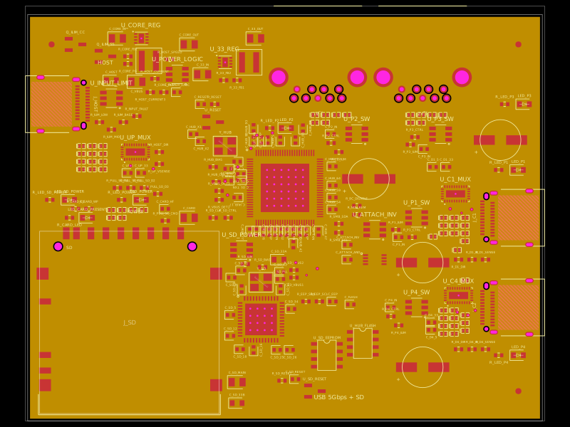 More from this authorgokul/usb3-sd-hubEngineering draft: four-layer, computer-powered USB 3 hub with one USB-C host socket, two USB-C and two USB-A accessory sockets, and a full-size SD slot. Board and three schematic previews are available. Routing and production checks are incomplete; not fabrication ready.
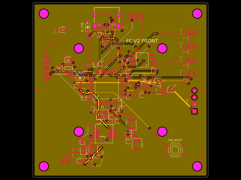 Discover something newmohan-bee/flight-controller-v2A 64 mm STM32F405 flight-controller PCB with ICM-42688 IMU, SPI flash, USB-C/ESD, battery buck and 3.3 V regulation, four motor outputs, service I/O, and PETG standoff mounting hardware.