astra/pd-power-supply
USB-PD Power Supply with RP2040 controller
- Version
- 1.1.6
- License
- unset
- Stars
- 0
scripts/audit-power.cjs
const fs=require('node:fs'),assert=require('node:assert/strict');
const rows=[];
assert.ok(!fs.readFileSync('build.log','utf8').includes('Async effect error'),'Build log contains an incomplete DRC effect');
for(const entry of ['board','index']){
 const d=JSON.parse(fs.readFileSync(`dist/${entry}/circuit.json`));
 assert.equal(d.filter(x=>x.type.includes('error')).length,0,`${entry}: DRC errors`);
 const src=n=>d.find(x=>x.type==='source_component'&&x.name===n);
 const pcb=n=>d.find(x=>x.type==='pcb_component'&&x.source_component_id===src(n)?.source_component_id);
 for(const n of ['J_PWR','J_DATA'])assert.equal(pcb(n).insertion_direction,'from_left');
 for(const n of ['J_LEVER'])assert.equal(pcb(n).insertion_direction,'from_bottom');
 for(const name of ['USB_PWR_ESCAPE_A','USB_PWR_ESCAPE_B','LOAD_IN_ESCAPE','LOAD_OUT_ESCAPE','LOAD_IN_FANOUT','LOAD_OUT_FANOUT','PD_RAW_TRUNK','PD_BUS_TRUNK','OUTPUT_BUS_TRUNK','VOUT_WAGO_TRUNK']){
  const s=d.find(x=>x.type==='source_trace'&&x.name===name);assert.ok(s,`${name}: missing source`);
  const t=d.find(x=>x.type==='pcb_trace'&&x.source_trace_id===s.source_trace_id);assert.ok(t,`${name}: missing copper`);
  const widths=t.route.filter(p=>p.route_type==='wire').map(p=>p.width);
  const expected=name.startsWith('USB_')?.5:name.endsWith('_ESCAPE')?.3:1.5;
  for(const w of widths)assert.ok(w>=expected-1e-8,`${name}: narrowed to ${w}`);
  let length=0;for(let i=1;i<t.route.length;i++)length+=Math.hypot(t.route[i].x-t.route[i-1].x,t.route[i].y-t.route[i-1].y);
  if(name==='LOAD_IN_ESCAPE'||name==='LOAD_OUT_ESCAPE')assert.ok(length<=2.151,`${name}: excessive narrow pad escape`);
  const routeVias=t.route.filter(p=>p.route_type==='via');
  const vias=routeVias.map(p=>d.find(v=>v.type==='pcb_via'&&v.pcb_trace_id===t.pcb_trace_id&&Math.hypot(v.x-p.x,v.y-p.y)<1e-6));
  assert.ok(vias.every(Boolean),`${name}: missing via record`);
  for(const v of vias){assert.ok(Math.abs(v.hole_diameter-.3)<1e-9);assert.ok(v.outer_diameter>=.8)}
  const r=0.0172*length/(expected*.035)+vias.length*0.0172*1.6/(Math.PI*.3*.025);
  if(entry==='board')rows.push({name,width:expected,length_mm:length,vias:vias.length,resistance_milliohm:r,endpoints:s.display_name});
 }
 const gnd=d.find(x=>x.type==='source_net'&&x.name==='GND');
 for(const layer of ['inner1','inner2']){
  const pour=d.find(x=>x.type==='pcb_copper_pour'&&x.layer===layer);
  assert.equal(pour.source_net_id,gnd.source_net_id);assert.ok(pour.brep_shape.outer_ring.vertices.length>3);
 }
}
const common=['USB_PWR_ESCAPE_A','LOAD_IN_ESCAPE','LOAD_OUT_ESCAPE','LOAD_IN_FANOUT','LOAD_OUT_FANOUT','PD_RAW_TRUNK','PD_BUS_TRUNK','OUTPUT_BUS_TRUNK'];
const sum=names=>names.reduce((a,n)=>a+rows.find(r=>r.name===n).resistance_milliohm,0);
const wago=sum([...common,'VOUT_WAGO_TRUNK']);
fs.writeFileSync('power-trace-audit.md',`# Revision 1.1.5 power copper audit\n\nGenerated from both compiled circuit JSON files. Widths below are actual copper widths, not only nominal net settings. Dedicated paths connect the USB power junction, fuse, eFuse, shunt and front WAGO connector. The maintained switch only controls EN; it is not in series with the output. Load current does not depend on the controller or sensor escape traces. The 0.3 mm QFN escape centerlines are now 2.15 mm, including 1.20 mm within the power land and 0.75 mm overlapping the 1.5 mm fanout. Only approximately 0.20 mm extends beyond the land before the wide copper begins (less than 0.25 mm at the edges). Previously the 0.3 mm routes were 4.02 and 5.49 mm long. The small fanout pads are copper junctions marked doNotPlace, not fitted parts.\n\n| Path | Width (mm) | Length (mm) | 0.3 mm drill / 0.8 mm pad vias | Estimated resistance (mΩ) |\n|---|---:|---:|---:|---:|\n${rows.map(r=>`| ${r.name} | ${r.width} | ${r.length_mm.toFixed(2)} | ${r.vias} | ${r.resistance_milliohm.toFixed(2)} |`).join('\n')}\n\nAssumes 35 µm copper, 20 °C copper resistivity 0.0172 Ω·mm²/m and 25 µm via plating through 1.6 mm. The calculation conservatively counts QFN land/trace overlaps twice and uses 0.3 mm for the entire pad escape. The table conservatively treats each USB escape as carrying the full load; both VBUS pad groups are connected to the junction. Estimated positive copper drop at 1 A is **${wago.toFixed(1)} mV to WAGO**, excluding the 50 mΩ shunt, fuse, eFuse, cable and ground return. Two inner GND pours connect the through-hole output/USB shell grounds; surface ground routes nominally use 1 mm and narrow for local pin escapes.\n\nTI recommends short power paths sized for at least twice the load and substantial copper at the IN/OUT pads: [TPS25947 layout guidance](https://www.ti.com/lit/ds/symlink/tps25947.pdf).\n\nZero compiled DRC errors in both entries. The audit asserts 1.5 mm dedicated trunks, 0.5 mm USB escapes, 0.3 mm QFN escapes capped at 2.15 mm centerline length and 1.5 mm fanouts, 0.3 mm power-via drills, two inner GND pours, and outward USB/output insertion directions. Width and resistance checks do not establish temperature rise or manufacturing readiness. Verify the stackup, thermal behavior, switching loops, sense pickup and physical switch fit on hardware.\n`);
console.log(`PASS: actual power trunks 1.5 mm; USB escapes 0.5 mm; ground planes; estimated positive copper drop ${wago.toFixed(1)} mV at 1 A.`);
Related Packages
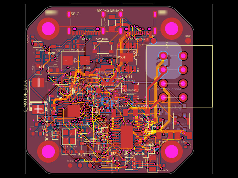 More from this authorastra/nema17-stepper-motor-controller-spring-clamp-rp2040A 4-layer RP2040 controller board that negotiates USB‑C PD motor power and drives a NEMA17 stepper via a DRV8825, with current sensing, thermal shutdown, RGB status LED, buzzer alarm, optional AS5600 encoder, protection/filtering, and test points.
 Similar packageaura/diy-power-delivery-triggerThis hardware design implements a USB Type-C port with supporting power management and signal conditioning components, including a USB-C connector, a FUSB302 USB-C port controller, ESD protection diodes, a buck converter for 3.3V power regulation, an STM32 microcontroller for control and processing, an RGB LED indicator, push button, terminal block connections, and associated filtering and support components.
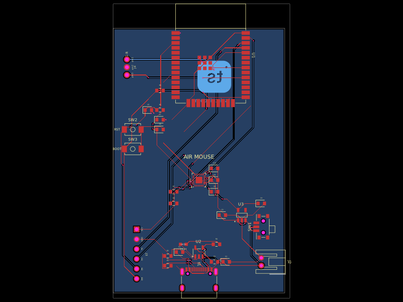 Discover something newhrithik18k/air-mouseA hardware component library defining footprints and 3D models for an ESP32 module, motion sensors, battery chargers, voltage regulator, connectors, switches, and status LED.