abse/rp2350-mcu-board
This code defines a compact, four-layer PCB hardware layout for the Raspberry Pi RP2350A microcontroller module, including the main IC, power regulation, USB-C connector, STM32-compatible headers, and associated passive components, with detailed component footprints, net connections, and copper pour zones for powering and ground references.
- Version
- 0.0.11
- License
- unset
- Stars
- 0
index.circuit.tsx
PCB
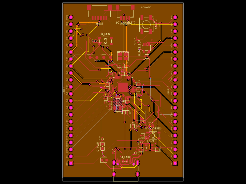
Schematic
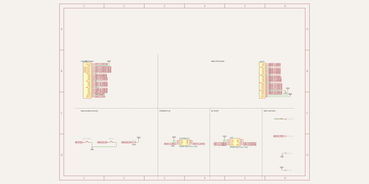
import { W25Q16JVUXIQ } from "./imports/W25Q16JVUXIQ"
import { SKRPACE010 } from "./imports/SKRPACE010"
import { TYPE_C_16PIN_2MD_073_ } from "./imports/TYPE_C_16PIN_2MD_073_"
import { AP2112K_3_3TRG1 } from "./imports/AP2112K_3_3TRG1"
import { XL_1608SURC_06 } from "./imports/XL_1608SURC_06"
import { XL_5050RGBC_2812B_S } from "./imports/XL_5050RGBC_2812B_S"
import { SN74AHCT1G125DBVR } from "./imports/SN74AHCT1G125DBVR"
import { SM04B_SRSS_TB_LF__SN_ } from "./imports/SM04B_SRSS_TB_LF__SN_"
import { SM06B_SRSS_TB_LF__SN_ } from "./imports/SM06B_SRSS_TB_LF__SN_"
import { RP2350AEssentialKiCadReference } from "./RP2350A_Essential_KiCad_Reference.circuit"
import { Fragment } from "react"

const gndLabel = { displayName: "GND", schDisplayLabel: "GND" } as const
const groundPlaneTraceProps = { ...gndLabel, thickness: "0.1mm" } as const
const v3v3Label = { displayName: "V3V3", schDisplayLabel: "V3V3" } as const
const vbusLabel = { displayName: "VBUS", schDisplayLabel: "VBUS" } as const
const denseTraceProps = { thickness: "0.1mm" } as const
const signalTraceProps = { thickness: "0.12mm" } as const
const powerTraceProps = { thickness: "0.3mm" } as const

const leftHeaderSignals = [
  "V3V3_EN",
  "V3V3",
  "GPIO29_ADC3",
  "GPIO28_ADC2",
  "GPIO27_ADC1",
  "GPIO26_ADC0",
  "GND",
  "GPIO25",
  "GPIO24",
  "GPIO23",
  "GPIO22",
  "GND",
  "GPIO21",
  "GPIO20",
  "GPIO19",
  "GND",
  "GPIO18",
  "GPIO17",
  "GPIO16",
  "RUN",
  "SWDIO",
  "SWCLK",
] as const

const rightHeaderSignals = [
  "GPIO0",
  "GPIO1",
  "GND",
  "GPIO2",
  "GPIO3",
  "GPIO4",
  "GPIO5",
  "GND",
  "GPIO6",
  "GPIO7",
  "GPIO8",
  "GPIO9",
  "GND",
  "GPIO10",
  "GPIO11",
  "GPIO12",
  "GPIO13",
  "GND",
  "GPIO14",
  "GPIO15",
  "V3V3",
  "VBUS",
] as const

const leftHeaderLabels = Object.fromEntries(
  leftHeaderSignals.map((signal, index) => [
    `pin${index + 1}`,
    signal === "GND" ? `GND_${index + 1}` : signal.replace("GPIO", "GP"),
  ]),
)

const rightHeaderLabels = Object.fromEntries(
  rightHeaderSignals.map((signal, index) => [
    `pin${index + 1}`,
    signal === "GND" ? `GND_${index + 1}` : signal.replace("GPIO", "GP"),
  ]),
)

/**
 * Standalone RP2350A USB-C development board.
 *
 * The RP2350A symbol and QFN-60 footprint are imported from JLCPCB part
 * C42411118. Its surrounding flash, crystal, reset, debug, and supply
 * topology follows Raspberry Pi's RP2350 hardware design guidance, with a
 * local 3.3 V regulator and physical headers for every GPIO and SWD signal.
 */
export const RP2350DevelopmentBoard = () => (
  <board
    title="RP2350A USB-C Development Board"
    width="44mm"
    height="64mm"
    layers={4}
    thickness="0.8mm"
    allowBlindAndBuriedVias={false}
    minTraceWidth="0.1mm"
    defaultTraceWidth="0.12mm"
    minViaHoleDiameter="0.2mm"
    minViaHoleEdgeToViaHoleEdgeClearance="0.2mm"
    minViaPadDiameter="0.45mm"
    autorouterVersion="beta_pipeline9"
    schAutoLayoutEnabled
  >
    <net name="GND" isGroundNet />
    <net name="VBUS" isPowerNet nominalTraceWidth="0.3mm" />
    <net name="V3V3" isPowerNet />
    <net name="USB_DP_OUT" />
    <net name="USB_DM_OUT" />
    {/* Ground pour clears the automatically routed copper on inner1. */}
    <copperpour
      name="GND_PLANE_INNER1"
      layer="inner1"
      connectsTo="net.GND"
      clearance="0.2mm"
      boardEdgeMargin="0.3mm"
      useThermalReliefs
    />
    {/* One automatic routing pass; no stored copper paths or routing cache. */}
    <autoroutingphase minTraceWidth="0.12mm" />

    <schematicsheet
      name="core"
      displayName="RP2350 MCU and GPIO"
      sheetIndex={0}
    >
      <schematicsection name="rp2350" displayName="RP2350A MCU" />
      <schematicsection name="left_header" displayName="Left GPIO Header" />
      <schematicsection name="right_header" displayName="Right GPIO Header" />
      <schematicsection name="controls" displayName="Reset and Boot Controls" />
      <schematicsection name="i2c" displayName="STEMMA QT I2C" />
      <schematicsection name="spi" displayName="JST-SH SPI" />
      <schematicsection name="debug" displayName="SWD Test Points" />
    </schematicsheet>

    <schematicsheet
      name="interfaces"
      displayName="Power, USB and Peripherals"
      sheetIndex={1}
    >
      <schematicsection name="power" displayName="Power Regulation" />
      <schematicsection name="decoupling" displayName="Supply Decoupling" />
      <schematicsection name="usb" displayName="USB-C Interface" />
      <schematicsection name="flash" displayName="QSPI Flash and Boot" />
      <schematicsection name="clock" displayName="12 MHz Clock" />
      <schematicsection name="status" displayName="Status and Test LEDs" />
    </schematicsheet>

    <RP2350AEssentialKiCadReference
      name="MCU_CORE"
      pcbX={0}
      pcbY={0}
      pcbRotation={180}
      noConnectUnusedPins={false}
    >
      {/* Keep the QSPI boot circuit in the MCU routing scope. */}
      <W25Q16JVUXIQ
        name="U2"
        schSheetName="interfaces"
        schSectionName="flash"
        pcbX={-6.5}
        pcbY={12}
        pcbRotation={270}
        schX={-1}
        schY={5.5}
        schHeight={1}
      />
      <SKRPACE010
        name="U_BOOTSEL"
        schSheetName="core"
        schSectionName="controls"
        schX={-12.56}
        schY={-6.5}
        pcbX={-11}
        pcbY={16.5}
        pcbRotation={180}
      />
      <resistor
        name="R_BOOT"
        resistance="10k"
        footprint="0402"
        supplierPartNumbers={{ jlcpcb: ["C25744"] }}
        schSheetName="interfaces"
        schSectionName="flash"
        schX={-4}
        schY={3.5}
        pcbX={-10}
        pcbY={13}
        pcbRotation={180}
      />
      <capacitor
        name="C_FLASH"
        capacitance="100nF"
        maxDecouplingTraceLength={5.5}
        footprint="0402"
        supplierPartNumbers={{ jlcpcb: ["C1525"] }}
        schSheetName="interfaces"
        schSectionName="flash"
        schX={2}
        schY={3.5}
        schOrientation="vertical"
        pcbX={-3.5}
        pcbY={13.25}
        pcbRotation={90}
      />
      <testpoint
        name="TP_SWCLK"
        footprintVariant="pad"
        padShape="circle"
        padDiameter="1.1mm"
        schSheetName="core"
        schSectionName="debug"
        schX={13}
        schY={-5.7}
        pcbX={9.5}
        pcbY={-12}
      />
      {/* BOOTSEL series protection; no manual copper path. */}
      <resistor
        name="R_BOOT_SERIES"
        resistance="1kohm"
        footprint="res_p0.8656mm_pw0.5657mm_ph0.54mm"
        supplierPartNumbers={{ jlcpcb: ["C106235"] }}
        tolerance="1%"
        schSheetName="interfaces"
        schSectionName="flash"
        pcbX={-7}
        pcbY={16.5}
      />
      <trace name="QSPI_SS" from=".U1 > .QSPI_SS" to=".U2 > .CS" {...denseTraceProps} />
      <trace name="QSPI_SD0" from=".U1 > .QSPI_SD0" to=".U2 > .pin5" {...denseTraceProps} />
      <trace name="QSPI_SD1" from=".U1 > .QSPI_SD1" to=".U2 > .pin2" {...denseTraceProps} />
      <trace name="QSPI_SD2" from=".U1 > .QSPI_SD2" to=".U2 > .pin3" {...denseTraceProps} />
      <trace name="QSPI_SD3" from=".U1 > .QSPI_SD3" to=".U2 > .pin7" {...denseTraceProps} />
      <trace name="QSPI_SCLK" from=".U1 > .QSPI_SCLK" to=".U2 > .CLK" {...denseTraceProps} />
      <trace name="FLASH_VCC" from=".U2 > .VCC" to="net.V3V3" />
      <trace name="FLASH_GND" from=".U2 > .GND" to="net.GND" thickness="0.1mm" />
      <trace name="FLASH_EP" from=".U2 > .EP" to="net.GND" thickness="0.1mm" />
      <trace name="C_FLASH_P" from=".C_FLASH > .pin1" to=".U2 > .VCC" thickness="0.1mm" />
      <trace name="C_FLASH_G" from=".C_FLASH > .pin2" to="net.GND" thickness="0.1mm" />
      <trace name="BOOT_PULLUP" from=".R_BOOT > .pin1" to=".U1 > .QSPI_SS" />
      <trace name="BOOT_PULLUP_3V3" from=".R_BOOT > .pin2" to="net.V3V3" />
      <trace name="BOOTSEL" from=".U_BOOTSEL > .pin1" to=".R_BOOT_SERIES > .pin1" />
      <trace name="BOOTSEL_PROTECTED" from=".R_BOOT_SERIES > .pin2" to=".U1 > .QSPI_SS" />
      <trace name="BOOTSEL_GND" from=".U_BOOTSEL > .pin3" to="net.GND" thickness="0.1mm" />
      <trace name="SWCLK_TEST" from=".U1 > .SWCLK" to=".TP_SWCLK > .pin1" />
    </RP2350AEssentialKiCadReference>

    <pinheader
      name="J_LEFT"
      pinCount={22}
      pitch="2.54mm"
      gender="male"
      footprint="pinrow22_p2.54mm"
      pinLabels={leftHeaderLabels}
      pcbPinLabels={leftHeaderLabels}
        pcbX={-19}
      pcbY={0}
      pcbRotation={90}
      schSheetName="core"
      schSectionName="left_header"
      schX={-12.5}
      schY={1.5}
      schWidth={1.055}
    />
    <pinheader
      name="J_RIGHT"
      pinCount={22}
      pitch="2.54mm"
      gender="male"
      footprint="pinrow22_p2.54mm"
      pinLabels={rightHeaderLabels}
        pcbX={19}
      pcbY={0}
      pcbRotation={90}
      schSheetName="core"
      schSectionName="right_header"
      schX={10}
      schY={1.5}
      schWidth={0.77}
    />

    <SKRPACE010 name="U_RUN" schSheetName="core" schSectionName="controls" schX={-9.44} schY={-6.5} pcbX={-6.4} pcbY={18} />

    {/* Feather-compatible STEMMA QT / Qwiic I2C port. */}
    <SM04B_SRSS_TB_LF__SN_
      name="J_STEMMA_QT"
      schSheetName="core"
      schSectionName="i2c"
      pcbX={0.8}
      pcbY={28.5}
      pcbRotation={180}
      schX={0}
      schY={-6.5}
    />
    <SM06B_SRSS_TB_LF__SN_
      name="J_SPI"
      schSheetName="core"
      schSectionName="spi"
      pcbX={-8.55}
      pcbY={28.5}
      pcbRotation={180}
      schX={6.5}
      schY={-6.5}
    />

    {/* USB-C receptacle, matching the Pico's USB 2.0 device-side topology. */}
    <TYPE_C_16PIN_2MD_073_
      name="J_USB"
      pinAttributes={{ B8: { doNotConnect: true }, A8: { doNotConnect: true } }}
      schSheetName="interfaces"
      schSectionName="usb"
      pcbX={1}
      pcbY={-28}
      schX={-11}
      schY={5.5}
    />

    <AP2112K_3_3TRG1
      name="U_3V3"
      schSheetName="interfaces"
      schSectionName="power"
      schHeight={0.6}
      schX={-10}
      schY={-4}
      pcbX={9.5}
      pcbY={-21}
    />

    <resistor name="R_LDO_EN" resistance="100k" footprint="0402" supplierPartNumbers={{ jlcpcb: ["C25741"] }} schSheetName="interfaces" schSectionName="power" schX={-7} schY={-4} pcbX={6.8} pcbY={-18.9} pcbRotation={90} />
    <resistor name="R_RUN" resistance="10k" footprint="0402" supplierPartNumbers={{ jlcpcb: ["C25744"] }} schSheetName="core" schSectionName="controls" schX={-6.5} schY={-6.5} pcbX={-10} pcbY={18} pcbRotation={90} />
    <resistor name="R_CC1" resistance="5.1k" footprint="0402" supplierPartNumbers={{ jlcpcb: ["C25905"] }} schSheetName="interfaces" schSectionName="usb" schX={-13} schY={3.5} pcbX={-3.2} pcbY={-22.8} />
    <resistor name="R_CC2" resistance="5.1k" footprint="0402" supplierPartNumbers={{ jlcpcb: ["C25905"] }} schSheetName="interfaces" schSectionName="usb" schX={-9.5} schY={3.5} pcbX={4.6} pcbY={-22.9} pcbRotation={270} />
    <resistor name="R_PWR_LED" resistance="1k" footprint="0402" supplierPartNumbers={{ jlcpcb: ["C11702"] }} schSheetName="interfaces" schSectionName="status" schX={-3} schY={-4} pcbX={-7.5} pcbY={-17.8} pcbRotation={90} />

    <XL_1608SURC_06
      name="D_PWR"
      color="red"
      schSheetName="interfaces"
      schSectionName="status"
      schX={0}
      schY={-4}
      schRotation={180}
      pcbX={-7.5}
      pcbY={-20.5}
      pcbRotation={90}
    />

    {/* 5 V addressable RGB test LED, level-shifted from RP2350 GPIO15. */}
    <SN74AHCT1G125DBVR
      name="U_RGB_BUF"
      schSheetName="interfaces"
      schSectionName="status"
      schHeight={0.6}
      schX={-4.96}
      schY={-6}
      pcbX={8.5}
      pcbY={15.5}
      pcbRotation={90}
    />
    <resistor
      name="R_RGB_DATA"
      resistance="330"
      footprint="0402"
      supplierPartNumbers={{ jlcpcb: ["C100375"] }}
      schSheetName="interfaces"
      schSectionName="status"
      schX={0.96}
      schY={-6}
      pcbX={5.5}
      pcbY={18}
      pcbRotation={90}
    />
    <XL_5050RGBC_2812B_S
      name="D_RGB"
      noConnect={["DO"]}
      schSheetName="interfaces"
      schSectionName="status"
      schX={4}
      schY={-6}
      pcbX={8.5}
      pcbY={24}
      pcbRotation={270}
    />

    <capacitor name="C_VBUS" capacitance="10uF" footprint="0603" supplierPartNumbers={{ jlcpcb: ["C19702"] }} schSheetName="interfaces" schSectionName="usb" schX={-7.5} schY={5.5} schOrientation="vertical" pcbX={-6.8} pcbY={-25.5} />
    {/* Explicit local limits include the short pad escape and ground-plane via.
        The original net-only regulator capacitors had no decoupling limit. */}
    <capacitor name="C_LDO_IN" capacitance="4.7uF" maxDecouplingTraceLength={2.5} footprint="0402" supplierPartNumbers={{ jlcpcb: ["C23733"] }} schSheetName="interfaces" schSectionName="power" schX={-13} schY={-4} schOrientation="vertical" pcbX={12.5} pcbY={-21.44} pcbRotation={90} />
    <capacitor name="C_LDO_OUT" capacitance="4.7uF" maxDecouplingTraceLength={2.5} footprint="0402" supplierPartNumbers={{ jlcpcb: ["C23733"] }} schSheetName="interfaces" schSectionName="power" schX={-7} schY={-5.5} schOrientation="vertical" pcbX={6.4} pcbY={-21.7} pcbRotation={180} />
    <capacitor name="C_RGB_BUF" capacitance="100nF" maxDecouplingTraceLength={5.5} footprint="0402" supplierPartNumbers={{ jlcpcb: ["C1525"] }} schSheetName="interfaces" schSectionName="status" schX={-4} schY={-8} schOrientation="vertical" pcbX={8.5} pcbY={12.4} pcbRotation={180} />
    <capacitor name="C_RGB" capacitance="100nF" maxDecouplingTraceLength={6.5} footprint="0402" supplierPartNumbers={{ jlcpcb: ["C1525"] }} schSheetName="interfaces" schSectionName="status" schX={4} schY={-8} schOrientation="vertical" pcbX={12} pcbY={24} pcbRotation={270} />

    <testpoint name="TP_SWDIO" footprintVariant="pad" padShape="circle" padDiameter="1.1mm" schSheetName="core" schSectionName="debug" schX={13} schY={-3.5} pcbX={-12} pcbY={12} />
    <testpoint name="TP_GND" footprintVariant="pad" padShape="circle" padDiameter="1.1mm" schSheetName="core" schSectionName="debug" schX={13} schY={-7.9} pcbX={-7} pcbY={12} />
    <testpoint name="TP_3V3" footprintVariant="pad" padShape="circle" padDiameter="1.1mm" schSheetName="core" schSectionName="debug" schX={13} schY={-10.1} pcbX={-4.5} pcbY={12} />

    {/* Board supplies feed the MCU's ordinary placement group. */}
    <trace name="LDO_VIN" from=".U_3V3 > .VIN" to=".J_USB > .A4B9" {...vbusLabel} {...powerTraceProps} />
    <trace name="LDO_ENABLE_PULLUP" from="net.VBUS" to=".R_LDO_EN > .pin1" {...vbusLabel} />
    <trace name="LDO_ENABLE" from=".R_LDO_EN > .pin2" to=".U_3V3 > .EN" thickness="0.12mm" />
    <trace name="LDO_GND" from=".U_3V3 > .GND" to=".J_RIGHT > .pin3" {...gndLabel} {...powerTraceProps} />
    <trace name="LDO_VOUT" from=".U_3V3 > .VOUT" to=".J_RIGHT > .pin21" {...v3v3Label} {...powerTraceProps} />
    <trace name="C_LDO_IN_P" from=".C_LDO_IN > .pin1" to=".U_3V3 > .VIN" {...vbusLabel} {...powerTraceProps} />
    <trace name="C_LDO_IN_G" from=".C_LDO_IN > .pin2" to="net.GND" {...groundPlaneTraceProps} />
    <trace name="C_LDO_OUT_P" from=".C_LDO_OUT > .pin1" to=".U_3V3 > .VOUT" {...v3v3Label} {...powerTraceProps} />
    <trace name="C_LDO_OUT_G" from=".C_LDO_OUT > .pin2" to="net.GND" {...groundPlaneTraceProps} />
    <trace name="PWR_LED_3V3" from=".U_3V3 > .VOUT" to=".R_PWR_LED > .pin1" {...v3v3Label} />
    <trace name="PWR_LED_D" from=".R_PWR_LED > .pin2" to=".D_PWR > .anode" />
    <trace name="PWR_LED_GND" from=".D_PWR > .cathode" to="net.GND" {...groundPlaneTraceProps} />
    <trace name="RGB_BUF_VBUS" from=".U_RGB_BUF > .VCC" to=".C_RGB_BUF > .pin1" {...vbusLabel} {...powerTraceProps} />
    <trace name="RGB_VBUS_DISTRIBUTION" from=".U_RGB_BUF > .VCC" to=".D_RGB > .VDD" {...vbusLabel} {...powerTraceProps} />
    <trace name="RGB_BUF_DECOUPLING_VBUS" from=".U_RGB_BUF > .VCC" to="net.VBUS" {...vbusLabel} />
    <trace name="RGB_BUF_GND" from=".U_RGB_BUF > .GND" to=".C_RGB_BUF > .pin2" {...gndLabel} thickness="0.1mm" />
    <trace name="RGB_BUF_OE" from=".U_RGB_BUF > .OE" to=".C_RGB_BUF > .pin2" {...gndLabel} thickness="0.1mm" />
    <trace name="RGB_BUF_DECOUPLING_GND" from=".C_RGB_BUF > .pin2" to="net.GND" {...groundPlaneTraceProps} />
    <trace name="RGB_GPIO15" from=".J_RIGHT > .pin20" to=".U_RGB_BUF > .A" />
    <trace name="RGB_BUFFERED_DATA" from=".U_RGB_BUF > .Y" to=".R_RGB_DATA > .pin1" />
    <trace name="RGB_DATA_IN" from=".R_RGB_DATA > .pin2" to=".D_RGB > .DI" />
    <trace name="RGB_VBUS" from=".D_RGB > .VDD" to=".C_RGB > .pin1" {...vbusLabel} {...powerTraceProps} />
    <trace name="RGB_DECOUPLING_VBUS" from=".D_RGB > .VDD" to=".J_RIGHT > .pin22" {...vbusLabel} {...powerTraceProps} />
    <trace name="RGB_GND" from=".D_RGB > .GND" to=".C_RGB > .pin2" {...gndLabel} {...powerTraceProps} />
    <trace name="RGB_DECOUPLING_GND" from=".D_RGB > .GND" to=".J_LEFT > .pin16" {...gndLabel} {...powerTraceProps} />
    {/* Reset, USB-C, and SWD connect to the ordinary MCU placement group. */}
    <trace name="RUN_PULLUP" from=".R_RUN > .pin1" to=".MCU_CORE .U1 > .RUN" />
    <trace name="RUN_PULLUP_3V3" from=".R_RUN > .pin2" to="net.V3V3" {...v3v3Label} />
    <trace name="RUN_SWITCH" from=".U_RUN > .pin1" to=".MCU_CORE .U1 > .RUN" />
    <trace name="RUN_SWITCH_GND" from=".U_RUN > .pin3" to="net.GND" {...groundPlaneTraceProps} />
    <trace name="VBUS_A" from=".J_USB > .A4B9" to="net.VBUS" {...vbusLabel} />
    <trace name="VBUS_B" from=".J_USB > .B4A9" to="net.VBUS" {...vbusLabel} />
    <trace name="C_VBUS_P" from=".C_VBUS > .pin1" to="net.VBUS" {...vbusLabel} />
    <trace name="C_VBUS_G" from=".C_VBUS > .pin2" to="net.GND" {...groundPlaneTraceProps} />
    <trace name="USB_DM_A" from=".J_USB > .A7" to="net.USB_DM_OUT" {...denseTraceProps} />
    <trace name="USB_DM_B" from=".J_USB > .B7" to="net.USB_DM_OUT" {...denseTraceProps} />
    <trace name="USB_DP_A" from=".J_USB > .A6" to="net.USB_DP_OUT" {...denseTraceProps} />
    <trace name="USB_DP_B" from=".J_USB > .B6" to="net.USB_DP_OUT" {...denseTraceProps} />
    <trace name="CC1" from=".J_USB > .A5" to=".R_CC1 > .pin1" />
    <trace name="CC2" from=".J_USB > .B5" to=".R_CC2 > .pin1" />
    <trace name="CC1_GND" from=".R_CC1 > .pin2" to="net.GND" {...groundPlaneTraceProps} />
    <trace name="CC2_GND" from=".R_CC2 > .pin2" to="net.GND" {...groundPlaneTraceProps} />
    <trace name="USB_GND_A" from=".J_USB > .A1B12" to="net.GND" {...groundPlaneTraceProps} />
    <trace name="USB_GND_B" from=".J_USB > .B1A12" to="net.GND" {...groundPlaneTraceProps} />
    <trace name="USB_SHIELD_1" from=".J_USB > .EH1" to="net.GND" {...groundPlaneTraceProps} />
    <trace name="USB_SHIELD_1_ALT" from=".J_USB > .pin13_alt1" to=".J_USB > .EH1" {...gndLabel} thickness="0.1mm" />
    <trace name="USB_SHIELD_2" from=".J_USB > .EH2" to="net.GND" {...groundPlaneTraceProps} />
    <trace name="USB_SHIELD_2_ALT" from=".J_USB > .pin14_alt1" to=".J_USB > .EH2" {...gndLabel} thickness="0.1mm" />
    <trace name="SWDIO" from=".J_LEFT > .pin21" to=".TP_SWDIO > .pin1" />
    <trace name="T_TP_GND" from=".TP_GND > .pin1" to="net.GND" {...groundPlaneTraceProps} />
    <trace name="T_TP_3V3" from=".TP_3V3 > .pin1" to="net.V3V3" {...v3v3Label} />
    {leftHeaderSignals.map((signal, index) => (
      <Fragment key={`left-${index + 1}`}>
        <trace
          name={`LEFT_${index + 1}_${signal}`}
          from={`.J_LEFT > .pin${index + 1}`}
          to={
            signal === "GND"
              ? "net.GND"
              : signal === "V3V3"
                ? "net.V3V3"
                : signal === "V3V3_EN"
                  ? ".U_3V3 > .EN"
                : `.MCU_CORE .U1 > .${signal}`
          }
          {...(signal === "GND"
            ? groundPlaneTraceProps
            : signal === "V3V3"
              ? v3v3Label
              : signalTraceProps)}
        />
      </Fragment>
    ))}

    {rightHeaderSignals.map((signal, index) => (
      <Fragment key={`right-${index + 1}`}>
        <trace
          name={`RIGHT_${index + 1}_${signal}`}
          from={`.J_RIGHT > .pin${index + 1}`}
          to={
            signal === "GND"
              ? "net.GND"
              : signal === "V3V3"
                ? "net.V3V3"
                : signal === "VBUS"
                  ? "net.VBUS"
                  : `.MCU_CORE .U1 > .${signal}`
          }
          {...(signal === "GND"
            ? groundPlaneTraceProps
            : signal === "V3V3"
              ? v3v3Label
              : signal === "VBUS"
                ? vbusLabel
                : signalTraceProps)}
        />
      </Fragment>
    ))}

    <trace name="STEMMA_QT_GND" from=".J_STEMMA_QT > .GND" to="net.GND" {...groundPlaneTraceProps} />
    <trace name="STEMMA_QT_3V3" from=".J_STEMMA_QT > .V3V3" to=".J_RIGHT > .pin21" {...v3v3Label} {...powerTraceProps} />
    <trace name="STEMMA_QT_SDA" from=".J_STEMMA_QT > .SDA" to=".MCU_CORE .U1 > .GPIO2" {...signalTraceProps} />
    <trace name="STEMMA_QT_SCL" from=".J_STEMMA_QT > .SCL" to=".MCU_CORE .U1 > .GPIO3" {...signalTraceProps} />
    <trace name="SPI_JST_GND" from=".J_SPI > .GND" to="net.GND" {...groundPlaneTraceProps} />
    <trace name="SPI_JST_3V3" from=".J_SPI > .V3V3" to=".J_STEMMA_QT > .V3V3" {...v3v3Label} {...powerTraceProps} />
    <trace name="SPI_JST_SCK" from=".J_SPI > .SCK" to=".MCU_CORE .U1 > .GPIO18" {...signalTraceProps} />
    <trace name="SPI_JST_MOSI" from=".J_SPI > .MOSI" to=".MCU_CORE .U1 > .GPIO19" {...signalTraceProps} />
    <trace name="SPI_JST_MISO" from=".J_SPI > .MISO" to=".MCU_CORE .U1 > .GPIO16" {...signalTraceProps} />
    <trace name="SPI_JST_CS" from=".J_SPI > .CS" to=".MCU_CORE .U1 > .GPIO17" {...signalTraceProps} />

    <silkscreentext text="RP2350A" fontSize="1mm" pcbX={0} pcbY={14} />
    <silkscreentext text="USB-C" fontSize="0.8mm" pcbX={1} pcbY={-26} />
    <silkscreentext text="PWR" fontSize="0.8mm" pcbX={-7.5} pcbY={-22} />
    <silkscreentext text="RGB GP15" fontSize="0.7mm" pcbX={8.5} pcbY={30.3} />
    <silkscreentext text="STEMMA QT" fontSize="0.65mm" pcbX={0.8} pcbY={24.2} />
    <silkscreentext text="SPI JST" fontSize="0.65mm" pcbX={-8.55} pcbY={24.2} />
  </board>
)

export default RP2350DevelopmentBoard
Related Packages
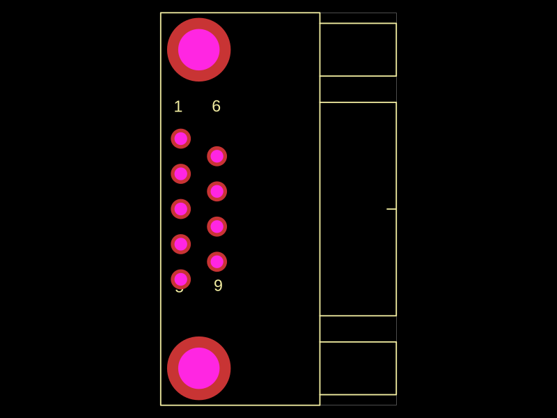 More from this authorabse/C75749Generated from JLCPCB part number C75749
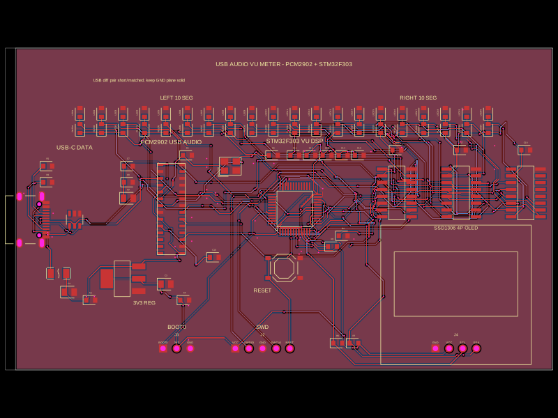 Similar packageimrishabh18/STM32F746G-DISCOThis code defines the hardware layout of a USB audio vu-meter circuit, including key components such as voltage regulators, microcontroller (STM32F303CCT6), audio codec (PCM2902), USB-Ethernet isolator, power regulation, reset switches, and associated passive components, with their physical footprints, pin configurations, and routing for PCB design.
 Discover something newbeaver/bq79600A 10mm x 10mm PCB with a BQ79600 battery monitor IC featuring 8 pins for power, discharge control, threshold detection, trigger, output, control, and reset.