abse/boostxl-bassensors
This code defines React components for various electronic hardware components such as LEDs and sensors, specifying their 3D models, footprints with SMT pads, silkscreen outlines, and pin labels for PCB integration.
- Version
- 1.0.3
- License
- unset
- Stars
- 0
index.circuit.tsx
PCB
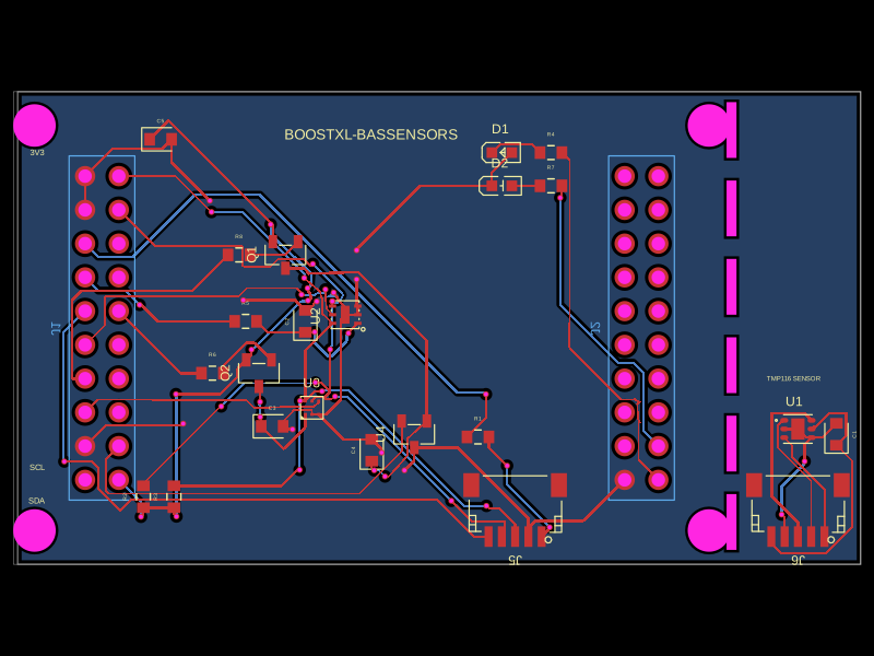
Schematic
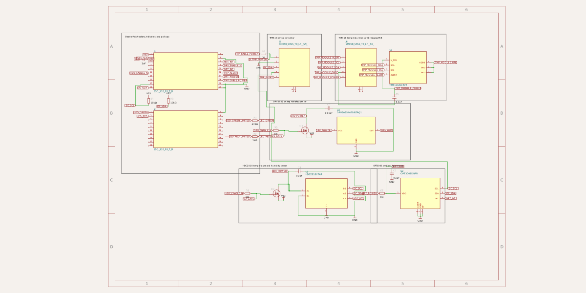
import { A_19_217_GHC_YR1S2_3T } from "./imports/A_19_217_GHC_YR1S2_3T/A_19_217_GHC_YR1S2_3T"
import { DRV5055A4EDBZRQ1 } from "./imports/DRV5055A4EDBZRQ1/DRV5055A4EDBZRQ1"
import { HDC2010YPAR } from "./imports/HDC2010YPAR/HDC2010YPAR"
import { KT_0603R } from "./imports/KT_0603R/KT_0603R"
import { OPT3001DNPR } from "./imports/OPT3001DNPR/OPT3001DNPR"
import { SI2323DS_T1_ES } from "./imports/SI2323DS_T1_ES/SI2323DS_T1_ES"
import { SM05B_SRSS_TB_LF__SN_ } from "./imports/SM05B_SRSS_TB_LF__SN_/SM05B_SRSS_TB_LF__SN_"
import { SSQ_110_03_T_D } from "./imports/SSQ_110_03_T_D/SSQ_110_03_T_D"
import { TMP116AIDRVR } from "./imports/TMP116AIDRVR/TMP116AIDRVR"
const N = {
V33: "net.V33",
GND: "net.GND",
I2C_SCL: "net.I2C_SCL",
I2C_SDA: "net.I2C_SDA",
DRV_OUT: "net.DRV_OUT",
DRV_ENABLE_N: "net.DRV_ENABLE_N",
DRV_POWER: "net.DRV_POWER",
HDC_ENABLE_N: "net.HDC_ENABLE_N",
HDC_POWER: "net.HDC_POWER",
HDC_INT: "net.HDC_INT",
OPT_POWER: "net.OPT_POWER",
OPT_INT: "net.OPT_INT",
TMP_CABLE_POWER: "net.TMP_CABLE_POWER",
TMP_ALERT: "net.TMP_ALERT",
TMP_MODULE_POWER: "net.TMP_MODULE_POWER",
TMP_MODULE_GND: "net.TMP_MODULE_GND",
TMP_MODULE_SCL: "net.TMP_MODULE_SCL",
TMP_MODULE_SDA: "net.TMP_MODULE_SDA",
TMP_MODULE_ALERT: "net.TMP_MODULE_ALERT",
LED_GREEN: "net.LED_GREEN",
LED_RED: "net.LED_RED",
} as const
const HEADER_SCH_PIN_STYLE = {
pin1: { marginTop: "0.05mm", marginBottom: "0.05mm" },
pin2: { marginTop: "0.05mm", marginBottom: "0.05mm" },
pin3: { marginTop: "0.05mm", marginBottom: "0.05mm" },
pin4: { marginTop: "0.05mm", marginBottom: "0.05mm" },
pin5: { marginTop: "0.05mm", marginBottom: "0.05mm" },
pin6: { marginTop: "0.05mm", marginBottom: "0.05mm" },
pin7: { marginTop: "0.05mm", marginBottom: "0.05mm" },
pin8: { marginTop: "0.05mm", marginBottom: "0.05mm" },
pin9: { marginTop: "0.05mm", marginBottom: "0.05mm" },
pin10: { marginTop: "0.05mm", marginBottom: "0.05mm" },
pin11: { marginTop: "0.05mm", marginBottom: "0.05mm" },
pin12: { marginTop: "0.05mm", marginBottom: "0.05mm" },
pin13: { marginTop: "0.05mm", marginBottom: "0.05mm" },
pin14: { marginTop: "0.05mm", marginBottom: "0.05mm" },
pin15: { marginTop: "0.05mm", marginBottom: "0.05mm" },
pin16: { marginTop: "0.05mm", marginBottom: "0.05mm" },
pin17: { marginTop: "0.05mm", marginBottom: "0.05mm" },
pin18: { marginTop: "0.05mm", marginBottom: "0.05mm" },
pin19: { marginTop: "0.05mm", marginBottom: "0.05mm" },
pin20: { marginTop: "0.05mm", marginBottom: "0.05mm" },
}
const SENSOR_SCH_PIN_STYLE = {
pin1: { marginTop: "0.1mm", marginBottom: "0.1mm" },
pin2: { marginTop: "0.1mm", marginBottom: "0.1mm" },
pin3: { marginTop: "0.1mm", marginBottom: "0.1mm" },
pin4: { marginTop: "0.1mm", marginBottom: "0.1mm" },
pin5: { marginTop: "0.1mm", marginBottom: "0.1mm" },
pin6: { marginTop: "0.1mm", marginBottom: "0.1mm" },
pin7: { marginTop: "0.1mm", marginBottom: "0.1mm" },
}
export default function Circuit() {
return (
<board
name="BOOSTXL_BASSENSORS"
pcbX="5.08mm"
width="63.5mm"
height="35.56mm"
outline={[
{ x: -26.67, y: -17.78 },
{ x: 36.83, y: -17.78 },
{ x: 36.83, y: 17.78 },
{ x: -26.67, y: 17.78 },
]}
solderMaskColor="red"
silkscreenColor="white"
defaultTraceWidth="0.2mm"
minViaHoleDiameter="0.3mm"
minViaPadDiameter="0.45mm"
autorouter={{
preset: "auto_local",
local: true,
traceClearance: "0.15mm",
}}
autorouterEffortLevel="5x"
>
<schematicsheet
name="BOOSTXL-BASSENSORS Complete Schematic"
displayName="BOOSTXL-BASSENSORS Complete Schematic"
sheetIndex={1}
/>
<group
name="BOOSTERPACK_INTERFACE_BLOCK"
schSheetName="BOOSTXL-BASSENSORS Complete Schematic"
schX={0.6}
schY={0}
pcbX={-5.08}
pcbY={0}
schMaxTraceDistance="0.8mm"
schTraceAutoLabelEnabled
>
<schematicsection
name="TI_REFERENCE_SCHEMATIC"
displayName=""
sectionTitleFontSize="0.18mm"
/>
<schematicrect schX={-10.0} schY={3.5} width="11.2mm" height="11.4mm" strokeWidth="0.03mm" color="#555555" />
<schematictext text="BoosterPack headers, indicators, and pull-ups" schX={-15.3} schY={8.9} fontSize={0.16} anchor="left" />
<SSQ_110_03_T_D
name="J1"
layer="bottom"
schSectionName="TI_REFERENCE_SCHEMATIC"
schX={-10.4}
schY={6.1}
schWidth="5.2mm"
schHeight="3mm"
schPinStyle={HEADER_SCH_PIN_STYLE}
schPinArrangement={{
leftSide: [1, 3, 5, 7, 9, 11, 13, 15, 17, 19],
rightSide: [2, 4, 6, 8, 10, 12, 14, 16, 18, 20],
}}
pcbX={-20.32}
pcbY={0}
pcbRotation={90}
noConnect={[
"pin2",
"pin5",
"pin7",
"pin9",
"pin13",
"pin15",
]}
connections={{
pin1: N.V33,
pin3: N.DRV_OUT,
pin4: N.GND,
pin6: N.HDC_INT,
pin8: N.DRV_ENABLE_N,
pin10: N.OPT_INT,
pin11: N.HDC_ENABLE_N,
pin12: N.TMP_ALERT,
pin14: N.OPT_POWER,
pin16: N.TMP_CABLE_POWER,
pin17: N.I2C_SCL,
pin18: N.GND,
pin19: N.I2C_SDA,
pin20: N.GND,
}}
/>
<SSQ_110_03_T_D
name="J2"
layer="bottom"
schSectionName="TI_REFERENCE_SCHEMATIC"
schX={-10.4}
schY={1.4}
schWidth="5.2mm"
schHeight="3mm"
schPinStyle={HEADER_SCH_PIN_STYLE}
schPinArrangement={{
leftSide: [1, 3, 5, 7, 9, 11, 13, 15, 17, 19],
rightSide: [2, 4, 6, 8, 10, 12, 14, 16, 18, 20],
}}
pcbX={20.32}
pcbY={0}
pcbRotation={90}
noConnect={[
"pin4",
"pin5",
"pin6",
"pin7",
"pin8",
"pin9",
"pin10",
"pin11",
"pin12",
"pin13",
"pin14",
"pin15",
"pin16",
"pin17",
"pin18",
"pin19",
"pin20",
]}
connections={{
pin1: N.LED_GREEN,
pin2: N.GND,
pin3: N.LED_RED,
}}
/>
<capacitor
name="C5"
schSectionName="TI_REFERENCE_SCHEMATIC"
schX={-13.8}
schY={7.1}
schRotation="0deg"
manufacturerPartNumber="C1608X7R1C105KT000N"
supplierPartNumbers={{ jlcpcb: ["C76617"] }}
capacitance="1uF"
footprint="0603"
pcbX={-15.9}
pcbY={14.2}
connections={{ pin1: N.V33, pin2: N.GND }}
/>
<resistor
name="R2"
schSectionName="TI_REFERENCE_SCHEMATIC"
schX={-13.4}
schY={3.7}
schRotation="270deg"
manufacturerPartNumber="CQ03WAF1002T5E"
supplierPartNumbers={{ jlcpcb: ["C516551"] }}
resistance="10kohm"
footprint="0603"
pcbX={-17.2}
pcbY={-12.7}
pcbRotation={90}
connections={{ pin1: N.V33, pin2: N.I2C_SCL }}
/>
<resistor
name="R3"
schSectionName="TI_REFERENCE_SCHEMATIC"
schX={-11.8}
schY={3.7}
schRotation="270deg"
manufacturerPartNumber="CQ03WAF1002T5E"
supplierPartNumbers={{ jlcpcb: ["C516551"] }}
resistance="10kohm"
footprint="0603"
pcbX={-14.9}
pcbY={-12.7}
pcbRotation={90}
connections={{ pin1: N.V33, pin2: N.I2C_SDA }}
/>
<A_19_217_GHC_YR1S2_3T
name="D1"
color="green"
schSectionName="TI_REFERENCE_SCHEMATIC"
schX={-6.6}
schY={2.1}
schRotation="0deg"
pcbX={9.8}
pcbY={13.2}
connections={{ pin1: "net.LED_GREEN_LIMITED", pin2: N.GND }}
/>
<resistor
name="R4"
schSectionName="TI_REFERENCE_SCHEMATIC"
schX={-4.8}
schY={2.1}
manufacturerPartNumber="0603WAF4700T5E"
supplierPartNumbers={{ jlcpcb: ["C23179"] }}
resistance="470ohm"
footprint="0603"
pcbX={13.5}
pcbY={13.2}
connections={{ pin1: "net.LED_GREEN_LIMITED", pin2: N.LED_GREEN }}
/>
<KT_0603R
name="D2"
color="red"
schSectionName="TI_REFERENCE_SCHEMATIC"
schX={-6.6}
schY={0.8}
schRotation="0deg"
pcbX={9.8}
pcbY={10.7}
connections={{ pin1: "net.LED_RED_LIMITED", pin2: N.GND }}
/>
<resistor
name="R7"
schSectionName="TI_REFERENCE_SCHEMATIC"
schX={-4.8}
schY={0.8}
manufacturerPartNumber="0603WAF1001T5E"
supplierPartNumbers={{ jlcpcb: ["C21190"] }}
resistance="1kohm"
footprint="0603"
pcbX={13.5}
pcbY={10.7}
connections={{ pin1: "net.LED_RED_LIMITED", pin2: N.LED_RED }}
/>
</group>
<group
name="TMP116_CONNECTOR_BLOCK"
schSheetName="BOOSTXL-BASSENSORS Complete Schematic"
schX={0}
schY={0}
pcbX={-5.08}
pcbY={0}
schMaxTraceDistance="0.8mm"
schTraceAutoLabelEnabled
>
<schematicsection name="TI_REFERENCE_SCHEMATIC" displayName="" sectionTitleFontSize="0.18mm" />
<schematicrect schX={-1.0} schY={6.4} width="4.4mm" height="5.4mm" strokeWidth="0.03mm" color="#555555" />
<schematictext text="TMP116 sensor connector" schX={-3.0} schY={8.8} fontSize={0.16} anchor="left" />
<resistor
name="R1"
schSectionName="TI_REFERENCE_SCHEMATIC"
schX={-3.5}
schY={7.5}
manufacturerPartNumber="0603WAF0000T5E"
supplierPartNumbers={{ jlcpcb: ["C21189"] }}
resistance="0ohm"
footprint="0603"
pcbX={8.0}
pcbY={-8.2}
connections={{ pin1: N.TMP_CABLE_POWER, pin2: "net.J5_TMP_POWER" }}
/>
<SM05B_SRSS_TB_LF__SN_
name="J5"
schSectionName="TI_REFERENCE_SCHEMATIC"
schX={-1}
schY={6.4}
schWidth="2.5mm"
schHeight="3.1mm"
schPinStyle={SENSOR_SCH_PIN_STYLE}
schPinArrangement={{ leftSide: [1, 2, 3, 4, 5], bottomSide: [6, 7] }}
pcbX={10.8}
pcbY={-13.7}
pcbRotation={180}
noConnect={["pin6", "pin7"]}
connections={{
pin1: "net.J5_TMP_POWER",
pin2: N.GND,
pin3: N.I2C_SDA,
pin5: N.TMP_ALERT,
}}
/>
<trace
name="J5_I2C_SCL"
from=".J5 > .pin4"
to={N.I2C_SCL}
schDisplayLabel="I2C_SCL"
/>
</group>
<group
name="TMP116_SENSOR_COUPON_BLOCK"
schSheetName="BOOSTXL-BASSENSORS Complete Schematic"
schX={0}
schY={0}
pcbX={-5.08}
pcbY={0}
schMaxTraceDistance="0.8mm"
schTraceAutoLabelEnabled
>
<schematicsection name="TI_REFERENCE_SCHEMATIC" displayName="" sectionTitleFontSize="0.18mm" />
<schematicrect schX={6.8} schY={6.4} width="9.0mm" height="5.4mm" strokeWidth="0.03mm" color="#555555" />
<schematictext text="TMP116 temperature sensor / breakaway PCB" schX={2.6} schY={8.8} fontSize={0.16} anchor="left" />
<SM05B_SRSS_TB_LF__SN_
name="J6"
schSectionName="TI_REFERENCE_SCHEMATIC"
schX={4.4}
schY={6.4}
schWidth="2.5mm"
schHeight="3.1mm"
schPinStyle={SENSOR_SCH_PIN_STYLE}
schPinArrangement={{ leftSide: [1, 2, 3, 4, 5], bottomSide: [6, 7] }}
pcbX={32.1}
pcbY={-13.7}
pcbRotation={180}
noConnect={["pin6", "pin7"]}
connections={{
pin1: N.TMP_MODULE_ALERT,
pin2: N.TMP_MODULE_SCL,
pin3: N.TMP_MODULE_SDA,
pin4: N.TMP_MODULE_GND,
pin5: N.TMP_MODULE_POWER,
}}
/>
<TMP116AIDRVR
name="U1"
schSectionName="TI_REFERENCE_SCHEMATIC"
schX={8.2}
schY={6.4}
schWidth="3mm"
schHeight="2.6mm"
schPinStyle={SENSOR_SCH_PIN_STYLE}
schPinArrangement={{
leftSide: [5, 6, 1, 3],
rightSide: [4, 2, 7],
}}
pcbX={32.1}
pcbY={-7.6}
pcbRotation={0}
connections={{
V_POS: N.TMP_MODULE_POWER,
SDA: N.TMP_MODULE_SDA,
SCL: N.TMP_MODULE_SCL,
ALERT: N.TMP_MODULE_ALERT,
ADD0: N.TMP_MODULE_GND,
GND: N.TMP_MODULE_GND,
PAD: N.TMP_MODULE_GND,
}}
/>
<capacitor
name="C1"
schSectionName="TI_REFERENCE_SCHEMATIC"
schX={7.1}
schY={3.95}
schRotation="270deg"
manufacturerPartNumber="GRM188R71E104KA01D"
supplierPartNumbers={{ jlcpcb: ["C77050"] }}
capacitance="0.1uF"
footprint="0603"
pcbX={35.0}
pcbY={-8.0}
pcbRotation={90}
connections={{ pin1: N.TMP_MODULE_POWER, pin2: N.TMP_MODULE_GND }}
/>
</group>
<group
name="DRV5055_BLOCK"
schSheetName="BOOSTXL-BASSENSORS Complete Schematic"
schX={0}
schY={0}
pcbX={-5.08}
pcbY={0}
schMaxTraceDistance="0.8mm"
schTraceAutoLabelEnabled
>
<schematicsection name="TI_REFERENCE_SCHEMATIC" displayName="" sectionTitleFontSize="0.18mm" />
<schematicrect schX={2.7} schY={1.2} width="11.4mm" height="4.6mm" strokeWidth="0.03mm" color="#555555" />
<schematictext text="DRV5055 analog Hall-effect sensor" schX={-2.7} schY={3.65} fontSize={0.16} anchor="left" />
<resistor
name="R8"
schSectionName="TI_REFERENCE_SCHEMATIC"
schX={-2.5}
schY={1.3}
manufacturerPartNumber="0603WAF0000T5E"
supplierPartNumbers={{ jlcpcb: ["C21189"] }}
resistance="0ohm"
footprint="0603"
pcbX={-10.0}
pcbY={5.5}
connections={{ pin1: N.DRV_ENABLE_N, pin2: "net.Q1_GATE" }}
/>
<SI2323DS_T1_ES
name="Q1"
schSectionName="TI_REFERENCE_SCHEMATIC"
schX={-0.3}
schY={1.3}
schRotation="0deg"
pcbX={-6.5}
pcbY={5.5}
pcbRotation={90}
connections={{
gate: "net.Q1_GATE",
source: N.V33,
drain: N.DRV_POWER,
}}
/>
<DRV5055A4EDBZRQ1
name="U4"
schSectionName="TI_REFERENCE_SCHEMATIC"
schX={4}
schY={1.3}
schWidth="3.1mm"
schHeight="2.2mm"
schPinArrangement={{ leftSide: [1], rightSide: [2], bottomSide: [3] }}
pcbX={3.2}
pcbY={-8.0}
pcbRotation={90}
connections={{ VCC: N.DRV_POWER, OUT: N.DRV_OUT, GND: N.GND }}
/>
<capacitor
name="C4"
schSectionName="TI_REFERENCE_SCHEMATIC"
schX={1.8}
schY={3.1}
schRotation="0deg"
manufacturerPartNumber="GRM188R71H103KA01D"
supplierPartNumbers={{ jlcpcb: ["C77053"] }}
capacitance="0.01uF"
footprint="0603"
pcbX={0}
pcbY={-9.2}
pcbRotation={90}
connections={{ pin1: N.DRV_POWER, pin2: N.GND }}
/>
</group>
<group
name="HDC2010_BLOCK"
schSheetName="BOOSTXL-BASSENSORS Complete Schematic"
schX={-2.0}
schY={0}
pcbX={-5.08}
pcbY={0}
schMaxTraceDistance="0.8mm"
schTraceAutoLabelEnabled
>
<schematicsection name="TI_REFERENCE_SCHEMATIC" displayName="" sectionTitleFontSize="0.18mm" />
<schematicrect schX={2.1} schY={-4.0} width="11.2mm" height="4.4mm" strokeWidth="0.03mm" color="#555555" />
<schematictext text="HDC2010 temperature and humidity sensor" schX={-3.2} schY={-1.55} fontSize={0.16} anchor="left" />
<resistor
name="R6"
schSectionName="TI_REFERENCE_SCHEMATIC"
schX={-2.8}
schY={-3.8}
manufacturerPartNumber="0603WAF0000T5E"
supplierPartNumbers={{ jlcpcb: ["C21189"] }}
resistance="0ohm"
footprint="0603"
pcbX={-12.0}
pcbY={-3.4}
connections={{ pin1: N.HDC_ENABLE_N, pin2: "net.Q2_GATE" }}
/>
<SI2323DS_T1_ES
name="Q2"
schSectionName="TI_REFERENCE_SCHEMATIC"
schX={-0.6}
schY={-3.8}
schRotation="0deg"
pcbX={-8.5}
pcbY={-3.4}
pcbRotation={90}
connections={{
gate: "net.Q2_GATE",
source: N.V33,
drain: N.HDC_POWER,
}}
/>
<HDC2010YPAR
name="U3"
schSectionName="TI_REFERENCE_SCHEMATIC"
schX={3.6}
schY={-3.8}
schWidth="3.4mm"
schHeight="2.4mm"
schPinStyle={SENSOR_SCH_PIN_STYLE}
schPinArrangement={{ leftSide: [2, 3], rightSide: [6, 1, 5], bottomSide: [4] }}
pcbX={-4.5}
pcbY={-6.0}
connections={{
A1: N.HDC_POWER,
B1: N.GND,
B2: N.I2C_SCL,
A2: N.I2C_SDA,
C2: N.HDC_INT,
C1: N.GND,
}}
/>
<capacitor
name="C3"
schSectionName="TI_REFERENCE_SCHEMATIC"
schX={1.4}
schY={-2}
schRotation="0deg"
manufacturerPartNumber="GRM188R71E104KA01D"
supplierPartNumbers={{ jlcpcb: ["C77050"] }}
capacitance="0.1uF"
footprint="0603"
pcbX={-7.5}
pcbY={-7.4}
connections={{ pin1: N.HDC_POWER, pin2: N.GND }}
/>
</group>
<group
name="OPT3001_BLOCK"
schSheetName="BOOSTXL-BASSENSORS Complete Schematic"
schX={-2.5}
schY={0}
pcbX={-5.08}
pcbY={0}
schMaxTraceDistance="0.8mm"
schTraceAutoLabelEnabled
>
<schematicsection name="TI_REFERENCE_SCHEMATIC" displayName="" sectionTitleFontSize="0.18mm" />
<schematicrect schX={10.7} schY={-4.0} width="6.0mm" height="4.4mm" strokeWidth="0.03mm" color="#555555" />
<schematictext text="OPT3001 ambient light sensor" schX={7.9} schY={-1.55} fontSize={0.16} anchor="left" />
<resistor
name="R5"
schSectionName="TI_REFERENCE_SCHEMATIC"
schX={8.6}
schY={-3.8}
manufacturerPartNumber="0603WAF0000T5E"
supplierPartNumbers={{ jlcpcb: ["C21189"] }}
resistance="0ohm"
footprint="0603"
pcbX={-9.5}
pcbY={0.5}
connections={{ pin1: N.OPT_POWER, pin2: "net.OPT_VDD" }}
/>
<OPT3001DNPR
name="U2"
schSectionName="TI_REFERENCE_SCHEMATIC"
schX={11.7}
schY={-3.8}
schWidth="3.2mm"
schHeight="2.5mm"
schPinStyle={SENSOR_SCH_PIN_STYLE}
schPinArrangement={{ leftSide: [1], rightSide: [4, 6, 5], bottomSide: [2, 3, 7] }}
pcbX={-2.0}
pcbY={1.0}
pcbRotation={90}
connections={{
VDD: "net.OPT_VDD",
SDA: N.I2C_SDA,
INT: N.OPT_INT,
ADDR: N.GND,
GND: N.GND,
EP: N.GND,
}}
/>
<trace
name="U2_I2C_SCL"
from=".U2 > .SCL"
to={N.I2C_SCL}
schDisplayLabel="I2C_SCL"
/>
<capacitor
name="C2"
schSectionName="TI_REFERENCE_SCHEMATIC"
schX={9.4}
schY={-2.2}
schRotation="270deg"
manufacturerPartNumber="GRM188R71E104KA01D"
supplierPartNumbers={{ jlcpcb: ["C77050"] }}
capacitance="0.1uF"
footprint="0603"
pcbX={-5.0}
pcbY={0.5}
pcbRotation={90}
connections={{ pin1: "net.OPT_VDD", pin2: N.GND }}
/>
</group>
<hole name="H1" diameter="3.2mm" pcbX={-30.48} pcbY={15.24} />
<hole name="H2" diameter="3.2mm" pcbX={20.32} pcbY={15.24} />
<hole name="H3" diameter="3.2mm" pcbX={-30.48} pcbY={-15.24} />
<hole name="H4" diameter="3.2mm" pcbX={20.32} pcbY={-15.24} />
{/* TI's TMP116 coupon is separated from the main PCB by routed perforation slots. */}
<cutout name="BREAK_SLOT_1" shape="rect" width="0.75mm" height="4.2mm" pcbX={22.02} pcbY={14.9} />
<cutout name="BREAK_SLOT_2" shape="rect" width="0.75mm" height="4.2mm" pcbX={22.02} pcbY={9.0} />
<cutout name="BREAK_SLOT_3" shape="rect" width="0.75mm" height="4.2mm" pcbX={22.02} pcbY={3.1} />
<cutout name="BREAK_SLOT_4" shape="rect" width="0.75mm" height="4.2mm" pcbX={22.02} pcbY={-2.8} />
<cutout name="BREAK_SLOT_5" shape="rect" width="0.75mm" height="4.2mm" pcbX={22.02} pcbY={-8.7} />
<cutout name="BREAK_SLOT_6" shape="rect" width="0.75mm" height="4.2mm" pcbX={22.02} pcbY={-14.6} />
<copperpour
name="GND_BOTTOM"
layer="bottom"
connectsTo={N.GND}
padMargin="0.25mm"
traceMargin="0.2mm"
boardEdgeMargin="0.3mm"
/>
<silkscreentext
text="BOOSTXL-BASSENSORS"
pcbX={-5.08}
pcbY={14.6}
fontSize="1.1mm"
/>
<silkscreentext text="3V3" pcbX={-30.28} pcbY={13.2} fontSize="0.62mm" />
<silkscreentext text="SCL" pcbX={-30.28} pcbY={-10.5} fontSize="0.62mm" />
<silkscreentext text="SDA" pcbX={-30.28} pcbY={-13} fontSize="0.62mm" />
<silkscreentext text="TMP116 SENSOR" pcbX={26.72} pcbY={-3.8} fontSize="0.5mm" />
</board>
)
}
Related Packages
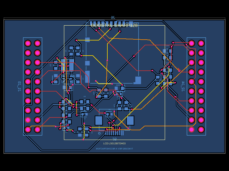 More from this authorabse/boostxl-sharp128This code defines a printed circuit board (PCB) with various surface-mount resistors, capacitors, inductors, and integrated circuits, including power management components and interface connectors, for a TI-based LCD and microSD module using 0603 and other package types.
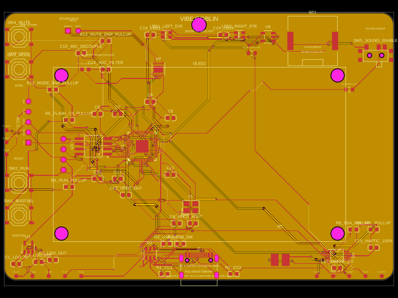 Similar packageAnasSarkiz/vibe_GoblinThese code snippets define various physical electronic components such as ICs, connectors, sensors, LEDs, and chips, specifying their pin layouts, footprint pads, silkscreen markings, courtyard outlines, and 3D CAD models for placement on PCB boards.
 Discover something newmohan-bee/stm32-mini-dev-board-v1-a-2A diagnostic STM32G031 development board with USB‑C 3.3V power, SWD/GPIO/UART/SPI headers, reset, potentiometer, buttons, LEDs, buzzer, I²C EEPROM, MCP23008 GPIO expansion, filtered inputs, and multiple I²C sensor ports.