MustafaMulla29/rp2040-bldc-motor-controller-new
A USB‑C PD–powered RP2040 BLDC motor controller PCB with 3.3 V logic, MCT8329A sensorless commutation, three MOSFET half-bridges, protected power switching, USB data, controls, and motor connectors.
- Version
- 0.3.82
- License
- unset
- Stars
- 0
scripts/check-routed.mjs
/** Re-run the installed native DRC against an actual, unedited build artifact. */
import { runAllChecks } from "@tscircuit/checks"
import { createHash } from "node:crypto"
import { mkdirSync, readFileSync, writeFileSync } from "node:fs"
import { dirname } from "node:path"

const input = process.argv[2] ?? "dist/index/circuit.json"
const raw = readFileSync(input)
const circuit = JSON.parse(raw)
let fresh = []
let checkExecutionError = null
try { fresh = await runAllChecks(circuit) }
catch (error) { checkExecutionError = String(error?.stack ?? error) }
const embeddedErrors = circuit.filter(x => x.type.endsWith("_error"))
const errors = fresh.filter(x => x.type.endsWith("_error"))
const warnings = fresh.filter(x => x.type.endsWith("_warning"))
const count = type => circuit.filter(x => x.type === type).length
const counts = items => items.reduce((r, x) => ({ ...r, [x.type]: (r[x.type] ?? 0) + 1 }), {})
const hasCopper = count("pcb_trace") > 0 && count("pcb_via") > 0
// Native inline pcbPath vias can ignore the board minima in the pinned core.
// Enforce exact dimensions, not just minima, independently of native DRC.
const viaDimensionViolations = circuit.filter(x => x.type === "pcb_via" &&
  (!Number.isFinite(x.hole_diameter) || !Number.isFinite(x.outer_diameter) ||
   Math.abs(x.hole_diameter - 0.3) > 1e-9 || Math.abs(x.outer_diameter - 0.45) > 1e-9))
  .map(x => ({ id: x.pcb_via_id, x: x.x, y: x.y,
    holeDiameter: x.hole_diameter, padDiameter: x.outer_diameter }))
// Verify the two connector domains in the compiled netlist, independently of
// routing completeness. A clean clearance check alone cannot detect miswiring.
const componentNames = new Map(circuit.filter(x => x.type === "source_component").map(x => [x.source_component_id, x.name]))
const netNames = new Map(circuit.filter(x => x.type === "source_net").map(x => [x.subcircuit_connectivity_map_key, x.name]))
const netNamesById = new Map(circuit.filter(x => x.type === "source_net").map(x => [x.source_net_id, x.name]))
const sourceTraces = new Map(circuit.filter(x => x.type === "source_trace").map(x => [x.source_trace_id, x]))
// L2 is the ground-reference layer. Through-via antipads are necessary, but
// non-ground tracks must not cut channels through that reference plane.
const groundPlaneViolations = circuit.filter(x => x.type === "pcb_trace").flatMap(trace => {
  const net = netNamesById.get(trace.connection_name) ??
    netNames.get(sourceTraces.get(trace.source_trace_id)?.subcircuit_connectivity_map_key)
  if (net === "GND") return []
  const hasL2Segment = trace.route.some((point, i, route) => {
    const next = route[i + 1]
    return point.route_type === "wire" && next?.route_type === "wire" &&
      point.layer === "inner1" && next.layer === "inner1" &&
      Math.hypot(point.x - next.x, point.y - next.y) > 1e-8
  })
  return hasL2Segment ? [{ trace: trace.pcb_trace_id, net: net ?? "UNKNOWN" }] : []
})
const pinNets = new Map(circuit.filter(x => x.type === "source_port").map(x =>
  [`${componentNames.get(x.source_component_id)}.${x.pin_number}`, netNames.get(x.subcircuit_connectivity_map_key) ?? null]))
const usbExpected = {
  "J1.6": "PROG_CC1", "J1.12": "PROG_CC2", "J1.15": "PROG_VBUS", "J1.16": "PROG_VBUS",
  "J1.7": "USB_DM", "J1.8": "USB_DP", "J1.9": "USB_DM", "J1.10": "USB_DP",
  "J19.6": "CC1", "J19.12": "CC2", "J19.15": "VBUS_RAW", "J19.16": "VBUS_RAW",
  "J19.5": null, "J19.7": null, "J19.8": null, "J19.9": null, "J19.10": null, "J19.11": null,
  "D5.1": "LOGIC_IN", "D5.2": "PROG_VBUS", "U5.12": "PROG_PRESENT",
  "R130.1": "PROG_CC1", "R130.2": "GND", "R131.1": "PROG_CC2", "R131.2": "GND",
  "R133.1": "PROG_VBUS", "R133.2": "PROG_PRESENT", "R134.1": "PROG_PRESENT", "R134.2": "GND",
  "C130.1": "PROG_VBUS", "C130.2": "GND",
}
const usbTopologyViolations = Object.entries(usbExpected)
  .filter(([pin, net]) => !pinNets.has(pin) || pinNets.get(pin) !== net)
  .map(([pin, expected]) => ({ pin, expected, actual: pinNets.get(pin) }))
for (const [name, resistance] of [["R130", 5100], ["R131", 5100], ["R133", 100000], ["R134", 100000]]) {
  const part = circuit.find(x => x.type === "source_component" && x.name === name)
  if (part?.resistance !== resistance) usbTopologyViolations.push({ component: name, expectedOhms: resistance, actualOhms: part?.resistance })
}
// Verify the hardware OFF function against compiled terminal connectivity.
// C&K JS202011JCQN: OFF closes 1-2 / 5-6; ON closes 2-3 / 6-7.
const powerExpected = {
  "R30.1":"VMOTOR", "F1.1":"PD9", "F1.2":"PD9_FUSED",
  "Q7.1":"PD9_FUSED", "Q7.2":"PD9_FUSED", "Q7.3":"PD9_FUSED", "Q7.4":"IDEAL_GATE", "Q7.5":"PD_LOAD",
  "U12.1":"IDEAL_VCAP", "U12.2":"GND", "U12.3":"PD9_FUSED", "U12.4":"PD_LOAD", "U12.5":"IDEAL_GATE", "U12.6":"PD9_FUSED",
  "C145.1":"IDEAL_VCAP", "C145.2":"PD9_FUSED", "C146.1":"PD9_FUSED", "C146.2":"GND", "D4.1":"PD_LOAD", "D4.2":"GND",
  "U11.8":"PD_LOAD", "U11.9":"PD_LOAD", "U11.10":"PD_LOAD",
  "U1.20":"PD_OK2_N", "U1.14":null, "U5.8":"PD_OK2_N",
  "R9.1":"V3V3", "R9.2":"PD_OK2_N", "R83.1":"PD_OK2_N", "R83.2":"PD_INHIBIT_B",
  "Q6.1":"PD_INHIBIT_B", "Q6.2":"GND",
  "U11.5":"VMOTOR", "U11.6":"VMOTOR", "U11.7":"VMOTOR",
  "U11.3":"POWER_SWITCH_EN", "U11.2":"GND", "U11.12":"GND", "U11.15":"GND",
  "U11.13":"POWER_CURRENT_LIMIT", "U11.1":null, "U11.4":null, "U11.11":null, "U11.14":null,
  "SW4.1":"GND", "SW4.2":"POWER_SWITCH_EN", "SW4.3":"POWER_ON_LEVEL",
  "SW4.5":"GND", "SW4.6":"ARM_BASE", "SW4.7":null,
  "D6.1":"VMOTOR", "D6.2":"PD_LOAD", "D7.1":"POWER_ON_LEVEL", "D7.2":"GND",
  "R140.1":"PD_LOAD", "R140.2":"POWER_ON_LEVEL", "R141.1":"POWER_ON_LEVEL", "R141.2":"GND",
  "R142.1":"POWER_CURRENT_LIMIT", "R142.2":"GND", "R143.1":"VMOTOR", "R143.2":"GND",
  "R144.1":"POWER_SWITCH_EN", "R144.2":"GND",
  "C140.1":"PD_LOAD", "C140.2":"GND", "C141.1":"PD_LOAD", "C141.2":"GND",
  "D2.2":"VBUS_RAW", "D2.1":"LOGIC_IN",
  "Q5.1":"ARM_BASE", "Q5.3":"MCT_DRVOFF", "Q5.2":"GND",
  "Q6.3":"ARM_BASE", "U7.5":"VMOTOR", "Q10.2":"VMOTOR", "Q12.2":"VMOTOR", "Q14.2":"VMOTOR",
}
const powerSwitchViolations = Object.entries(powerExpected)
  .filter(([pin, net]) => !pinNets.has(pin) || pinNets.get(pin) !== net)
  .map(([pin, expected]) => ({pin,expected,actual:pinNets.get(pin)}))
for (const [name,value] of [["R140",10000],["R141",22000],["R142",1500],["R143",10000],["R144",100000]]) {
  const p=circuit.find(x=>x.type==='source_component' && x.name===name)
  if(p?.resistance!==value)powerSwitchViolations.push({component:name,expectedOhms:value,actualOhms:p?.resistance})
}
const powerModeChecks = {
  off: {enableGrounded:pinNets.get('SW4.1')==='GND' && pinNets.get('SW4.2')===pinNets.get('U11.3'),
    armGrounded:pinNets.get('SW4.5')==='GND' && pinNets.get('SW4.6')===pinNets.get('Q5.1')},
  on: {enableBiased:pinNets.get('SW4.3')===pinNets.get('R141.1'), armClampReleased:pinNets.get('SW4.7')===null},
  offAdcIsolated:pinNets.get('R30.1')==='VMOTOR' && pinNets.get('R30.1')!==pinNets.get('F1.2'),
  usbProgrammingPreserved:pinNets.get('D5.2')==='PROG_VBUS' && pinNets.get('D5.1')==='LOGIC_IN',
}
for (const name of ["U8","U9","Q3","Q20","Q21","L2","J8","J13","J15","J16","R132"]) {
  if ([...componentNames.values()].includes(name)) powerSwitchViolations.push({component:name,expected:"battery/charger part removed"})
}
for (const name of [...netNames.values()]) {
  if (/^(BMS_|CHG_|BAL[123]$|BNEG$|VBAT|BAT_POS_RAW|CHARGE_ENABLE$|USB_INHIBIT_B$)/.test(name))
    powerSwitchViolations.push({net:name,expected:"no battery or USB-present inhibit nets"})
}
const connectorExpected = {
  "J10.1": "PHASE_U", "J10.2": "PHASE_U", "J11.1": "PHASE_V", "J11.2": "PHASE_V", "J12.1": "PHASE_W", "J12.2": "PHASE_W",
  "RV1.1": "GND", "RV1.2": "THROTTLE_IN", "RV1.3": "V3V3", "RV1.4": null, "RV1.5": null,
  "SW1.1": "BOOTSEL", "SW1.2": "BOOTSEL", "SW1.3": "GND", "SW1.4": "GND",
  "SW2.1": "RUN", "SW2.2": "RUN", "SW2.3": "GND", "SW2.4": "GND",
  "SW3.1": "ARM_REQUEST_N", "SW3.2": "ARM_REQUEST_N", "SW3.3": "GND", "SW3.4": "GND",
  ...Object.fromEntries(Object.values(JSON.parse(readFileSync(new URL('../circuit/service-pads.json',import.meta.url),'utf8'))).flat().map(p=>[`${p.name}.1`,p.net])),
}
const connectorViolations = Object.entries(connectorExpected)
  .filter(([pin, net]) => pinNets.get(pin) !== net)
  .map(([pin, expected]) => ({ pin, expected, actual: pinNets.get(pin) }))
for (const [name, mpn] of [["J10", "24.243.4"], ["J11", "24.243.4"], ["J12", "24.243.4"]]) {
  const part = circuit.find(x => x.type === "source_component" && x.name === name)
  if (part?.manufacturer_part_number !== mpn) connectorViolations.push({ component: name, expectedMpn: mpn })
}
const pcbPart = name => circuit.find(x => x.type === "pcb_component" && componentNames.get(x.source_component_id) === name)
const newParts = [
  ["SW4","JS202011JCQN","C221665"], ["U11","TPS1H100AQPWPRQ1","C478465"],
  ["D6","SS54","C22452"], ["D7","BZT52C4V7","C2116"],
  ...["SW1","SW2","SW3"].map(name=>[name,"TS-1187A-B-A-B","C318884"]),
  ["RV1","RK09K1130A8G","C470294"],
]
for (const [name,mpn,supplier] of newParts) {
  const part=pcbPart(name)
  const source=circuit.find(x=>x.type==='source_component' && x.name===name)
  const model=circuit.find(x=>x.type==='cad_component' && x.pcb_component_id===part?.pcb_component_id)
  const courtyard=circuit.find(x=>x.type.startsWith('pcb_courtyard_') && x.pcb_component_id===part?.pcb_component_id)
  if(source?.manufacturer_part_number!==mpn || source?.supplier_part_numbers?.jlcpcb?.[0]!==supplier || !model?.model_obj_url || !model?.model_step_url || !courtyard)
    connectorViolations.push({component:name,expected:`${mpn} / ${supplier}, CAD models and courtyard`})
}
for(const name of ["J2","J3","J4","J5","J6","J7","J17","J18"]) if(pcbPart(name)) connectorViolations.push({component:name,expected:'removed bare pin header'})
for(const source of circuit.filter(x=>x.type==='source_component' && x.ftype==='simple_test_point')) {
 const part=pcbPart(source.name)
 const pads=circuit.filter(x=>x.type==='pcb_smtpad' && x.pcb_component_id===part.pcb_component_id)
 const paste=circuit.filter(x=>x.type==='pcb_solder_paste' && x.pcb_component_id===part.pcb_component_id)
 if(pads.length!==1 || pads[0].shape!=='circle' || Math.abs(pads[0].radius-.75)>1e-6 || pads[0].is_covered_with_solder_mask || paste.length)
  connectorViolations.push({component:source.name,expected:'one exposed 1.5 mm copper pad, no solder paste'})
}
const outline = circuit.find(x => x.type === "pcb_board")
const leftEdge = (outline?.center?.x ?? 0) - outline.width / 2
for (const name of ["J1", "J19"]) {
  const part = pcbPart(name)
  if (!part?.cable_insertion_center || part.cable_insertion_center.x >= leftEdge || part.rotation !== 270)
    connectorViolations.push({ component: name, expected: "USB cable entry facing the left board edge" })
}
for (const [name, direction] of [["J10", "from_top"], ["J11", "from_top"], ["J12", "from_top"]]) {
  if (pcbPart(name)?.insertion_direction !== direction) connectorViolations.push({ component: name, expectedInsertionDirection: direction })
}
// C7437324's raised circular mating lip is on supplier-model +X, not its rear
// face at -X. Check physical CAD rotation too: insertion metadata alone could
// falsely claim outward access on a backwards footprint.
const topEdge = (outline.center?.y ?? 0) + outline.height / 2
for (const name of ["J10", "J11", "J12"]) {
  const part = pcbPart(name)
  const cad = circuit.find(x => x.type === "cad_component" && x.pcb_component_id === part?.pcb_component_id)
  const frontY = cad && cad.position.y + (13.25 - cad.model_origin_position.x) * (cad.model_unit_to_mm_scale_factor ?? 1)
  if (part?.rotation !== 90 || cad?.rotation?.z !== 90 || !cad.model_obj_url?.includes("C7437324") || !(frontY > topEdge))
    connectorViolations.push({ component: name, expected: "Supplier +X circular socket mouth facing out past the top board edge" })
}
// Top-only assembly is a physical placement requirement, not a BOM omission.
for (const part of circuit.filter(x => x.type === "pcb_component" && componentNames.has(x.source_component_id))) {
  if (part.layer !== "top") connectorViolations.push({ component: componentNames.get(part.source_component_id), expectedAssemblyLayer: "top", actual: part.layer })
}
// HRO manufacturer land-pattern dimensions, checked on compiled copper.
const usbFootprintViolations = []
const near = (a, b) => Number.isFinite(a) && Math.abs(a - b) < 1e-6
for (const name of ["J1", "J19"]) {
  const part = pcbPart(name)
  const pads = circuit.filter(x => x.type === "pcb_smtpad" && x.pcb_component_id === part.pcb_component_id)
  const slots = circuit.filter(x => x.type === "pcb_plated_hole" && x.pcb_component_id === part.pcb_component_id)
  const pegs = circuit.filter(x => x.type === "pcb_hole" && x.pcb_component_id === part.pcb_component_id)
  const check = (ok, detail) => { if (!ok) usbFootprintViolations.push({ component: name, detail }) }
  check(pads.length === 12 && slots.length === 4 && pegs.length === 2, "12 signal/power lands, four shell slots and two locating holes")
  for (const p of pads) {
    const pin = Number(p.port_hints.find(h => /^pin\d+$/.test(h))?.slice(3))
    const localX = pin <= 12 ? -1.75 + (pin - 5) * 0.5 : ({13:-3.2,14:3.2,15:2.4,16:-2.4})[pin]
    check(near(p.width, 1.14) && near(p.height, pin <= 12 ? 0.3 : 0.6) &&
      near(p.x, part.display_offset_x + 1.9755672) && near(p.y, part.display_offset_y - localX), `Land pin${pin}: manufacturer dimensions and pitch`)
  }
  for (const p of slots) {
    const pin = Number(p.port_hints.find(h => /^pin\d+$/.test(h))?.slice(3))
    const rear = [1,4].includes(pin)
    check(near(p.hole_width, 0.6) && near(p.hole_height, rear ? 1.7 : 1.4) &&
      near(p.outer_width, 0.9) && near(p.outer_height, rear ? 2 : 1.7) &&
      near(p.x, part.display_offset_x + (rear ? 1.4055672 : -2.7744328)) &&
      near(Math.abs(p.y - part.display_offset_y), 4.325), `Shell slot pin${pin}: manufacturer dimensions and location`)
  }
  for (const p of pegs) check(near(p.hole_diameter, 0.6) && near(p.x, part.display_offset_x + 0.9055672) && near(Math.abs(p.y - part.display_offset_y), 2.89), "Locating hole dimensions and position")
  check(near(part.display_offset_x + 1.4055672 - 5.79, leftEdge), "Manufacturer PCB edge datum")
}
const report = {
  checkedAt: new Date().toISOString(),
  input,
  circuitSha256: createHash("sha256").update(raw).digest("hex"),
  status: hasCopper && !embeddedErrors.length && !errors.length &&
    !viaDimensionViolations.length && !groundPlaneViolations.length && !usbTopologyViolations.length && !powerSwitchViolations.length && !connectorViolations.length && !usbFootprintViolations.length && !checkExecutionError ? "PASS" : "FAIL",
  checkExecutionError,
  hasRoutedCopper: hasCopper,
  pcbTraces: count("pcb_trace"),
  pcbVias: count("pcb_via"),
  exactViaDimensionsMm: { hole: 0.3, pad: 0.45 },
  viaDimensionViolations,
  groundPlaneViolations,
  usbTopologyViolations,
  powerSwitchViolations,
  powerModeChecks,
  connectorViolations,
  usbFootprintViolations,
  embeddedErrorCounts: counts(embeddedErrors),
  freshErrorCounts: counts(errors),
  freshWarningCounts: counts(warnings),
  embeddedErrors,
  errors,
  warnings,
  limitations: "Installed tscircuit CAD checks only; does not certify electrical behavior, current capacity, thermal performance, USB signal integrity or fabrication readiness.",
}
const output = process.argv[3] ?? ".tscircuit/checks/drc.json"
mkdirSync(dirname(output), { recursive: true })
writeFileSync(output, JSON.stringify(report, null, 2) + "\n")
console.log(JSON.stringify({ ...report, embeddedErrors: undefined, errors: undefined, warnings: undefined }, null, 2))
process.exitCode = report.status === "PASS" ? 0 : 1
Related Packages
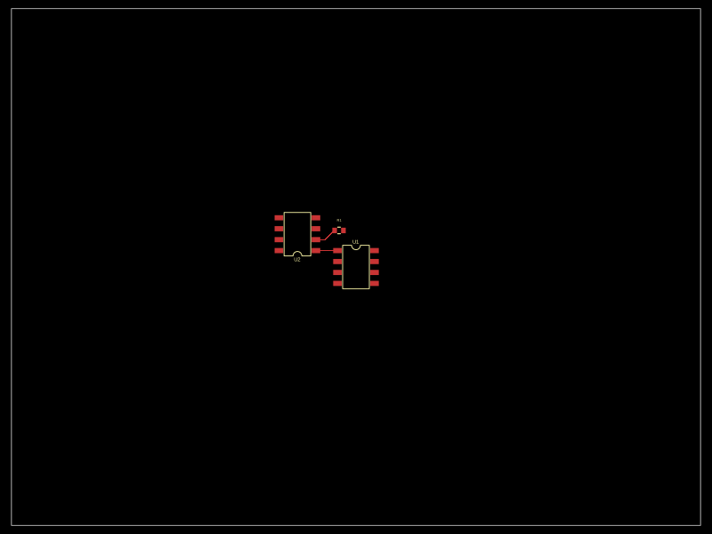 More from this authorMustafaMulla29/auto-placeA small PCB featuring two SOIC-8 ICs interconnected with a resistor.
 Similar packageimrishabh18/rp2040-motor-controllerAn RP2040-based NEMA17 stepper-motor controller with USB-C programming and PD motor-power negotiation, DRV8825 dual H-bridge drive, current/temperature telemetry, protected power filtering, status RGB LED, buzzer alarm, and optional magnetic encoder.
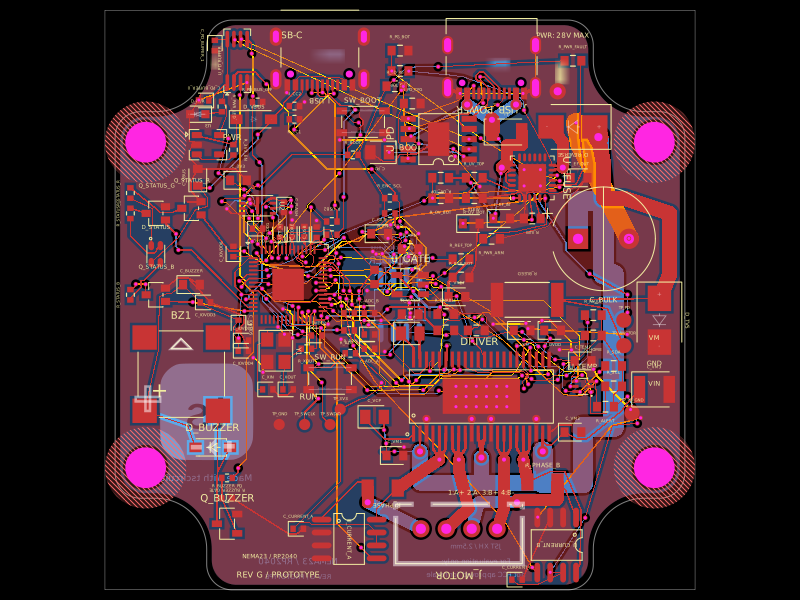 Discover something newimrishabh18/nema-23-stepper-controllerA curved NEMA23 rear-mount PCB combining an RP2040 controller, USB-C/USB-PD power input and protection, DRV8452 dual-winding stepper driver, current sensing, thermal interlock, status RGB LED, buzzer, and optional I²C encoder interface.