Devesh36/usb-c-phone-stand-light
A 3D-printed tilted phone stand integrating USB‑C PD power, a Qi wireless charging coil with magnetic alignment ring, indicator LEDs/light pipes, control and protection PCBs, wiring, fasteners, and rubber feet.
- Version
- 0.0.6
- License
- unset
- Stars
- 0
lighting-board.tsx
import { Fragment } from "react";

export function WireHeader({name,x,y,pins=2,labels,schX=0,schY=0}:{name:string;x:number;y:number;pins?:number;labels?:Record<string,string>;schX?:number;schY?:number}){
 return <pinheader name={name} pinCount={pins} pinLabels={labels} pcbX={x} pcbY={y} schX={schX} schY={schY}
 manufacturerPartNumber={pins===2?"Solder wire pads, 5.08mm":"Solder wire pads, 2.54mm"}
 footprint={<footprint>{Array.from({length:pins},(_,i)=><Fragment key={i}><platedhole portHints={[`pin${i+1}`]} pcbY={((pins-1)/2-i)*(pins===2?5.08:2.54)} shape="circle" holeDiameter={pins===2?1.2:0.9} outerDiameter={pins===2?2.4:1.8}/></Fragment>)}</footprint>}
 cadModel={null}/>;
}

export default function LightingBoard(){
 return <board name="POWER" width={72} height={28} thickness={1.6} mountedTo="BASE.pcb" mountGap={0.2} routingDisabled minTraceToPadEdgeClearance="0.2mm">
  <WireHeader name="J_USB" x={-27} y={0} schX={-8} labels={{pin1:"5V",pin2:"GND"}}/>
  <WireHeader name="J_QI" x={-7} y={0} schX={-1} schY={4} labels={{pin1:"5V_QI",pin2:"GND"}}/>
  <WireHeader name="J_STATUS" x={10} y={6} schX={1} schY={-3} labels={{pin1:"LED_A_3V3",pin2:"GND"}}/>
  <WireHeader name="J_PANEL" x={26} y={0} pins={4} schX={8} labels={{pin1:"UV_A",pin2:"UV_K",pin3:"IR_A",pin4:"IR_K"}}/>
  <fuse name="F_QI" footprint="1812" pcbX={-17} pcbY={6} currentRating="2A" voltageRating={6} manufacturerPartNumber="MF-MSMF200-2" schX={-5} schY={4}/>
  <fuse name="F_LED" footprint="1812" pcbX={-17} pcbY={-7} currentRating="250mA" voltageRating={16} manufacturerPartNumber="MF-MSMF025-2" schX={-5} schY={-1}/>
  <resistor name="R_UV" resistance="1kohm" footprint="0805" pcbX={5} pcbY={-7} schX={1} schY={0} manufacturerPartNumber="RC0805FR-071KL"/>
  <resistor name="R_IR" resistance="470ohm" footprint="0805" pcbX={19} pcbY={7} schX={4} schY={-3} manufacturerPartNumber="RC0805FR-07470RL"/>
  <capacitor name="C1" manufacturerPartNumber="GRM21BR61C475KA73L" capacitance="4.7uF" maxVoltageRating={16} footprint="0805" pcbX={-3} pcbY={-7} pcbRotation={90} schX={-2} schY={-2}/>
  <net name="GND" isGroundNet connectsTo={["J_USB.pin2","J_QI.pin2","J_STATUS.pin2","J_PANEL.pin2","J_PANEL.pin4","C1.pin2"]}/>
  <trace name="J_USB_pin1_TO_F_QI_pin1" from="J_USB.pin1" to="F_QI.pin1" thickness={1} pcbPath={["J_USB.pin1",{x:0,y:6},"F_QI.pin1"]}/>
  <trace name="F_QI_pin2_TO_J_QI_pin1" from="F_QI.pin2" to="J_QI.pin1" thickness={1} pcbPath={["F_QI.pin2",{x:10,y:0},"J_QI.pin1"]}/>
  <trace name="J_USB_pin1_TO_F_LED_pin1" from="J_USB.pin1" to="F_LED.pin1" thickness={0.5} pcbPath={["J_USB.pin1",{x:-4,y:2.54},{x:-4,y:-7},"F_LED.pin1"]}/>
  <trace name="F_LED_pin2_TO_R_UV_pin1" from="F_LED.pin2" to="R_UV.pin1" thickness={0.3} pcbPath={["F_LED.pin2",{x:6,y:0},{x:6,y:-4},{x:21.025,y:-4},"R_UV.pin1"]}/>
  <trace name="F_LED_pin2_TO_C1_pin1" from="F_LED.pin2" to="C1.pin1" thickness={0.3} pcbPath={["F_LED.pin2",{x:6,y:0},{x:6,y:-4},{x:14,y:-4},"C1.pin1"]}/>
  <trace name="R_UV_pin2_TO_J_PANEL_pin1" from="R_UV.pin2" to="J_PANEL.pin1" thickness={0.3} pcbPath={["R_UV.pin2",{x:13,y:0},{x:13,y:10.81},"J_PANEL.pin1"]}/>
  <trace name="J_STATUS_pin1_TO_R_IR_pin1" from="J_STATUS.pin1" to="R_IR.pin1" thickness={0.25} pcbPath={["J_STATUS.pin1",{x:4,y:2.54},"R_IR.pin1"]}/>
  <trace name="R_IR_pin2_TO_J_PANEL_pin3" from="R_IR.pin2" to="J_PANEL.pin3" thickness={0.25} pcbPath={["R_IR.pin2",{x:11,y:0},{x:11,y:-8.27},"J_PANEL.pin3"]}/>
  <via name="C_GND" pcbX={-1} pcbY={-6} holeDiameter={0.3} outerDiameter={0.6} connectsTo="net.GND"/>
  <trace name="C1_pin2_TO_C_GND_top" from="C1.pin2" to="C_GND.top" pcbPath={["C1.pin2","C_GND.top"]}/>
  <copperpour name="GND_PLANE" layer="bottom" connectsTo="net.GND" useThermalReliefs={false} clearance={0.3} boardEdgeMargin={0.6}/>
  {[-31,31].flatMap(x=>[-10,10].map(y=><Fragment key={`${x}_${y}`}><hole name={`M_${x}_${y}`} pcbX={x} pcbY={y} diameter={2.2}/></Fragment>))}
  <silkscreentext text="USB TO QI" pcbX={-13} pcbY={11} fontSize={0.9}/>
  <silkscreentext text="POWER / CHARGE" pcbX={17} pcbY={-11} fontSize={0.7}/>
 </board>
}
Related Packages
 More from this authorDevesh36/red-accent-light-led-rotation-reproA 12V PCB red accent light using an LM317 constant-current driver to power two series high-power LEDs at 0° and 45°, with Schottky reverse-polarity protection, filtering capacitors, thermal vias/planes, and test points.
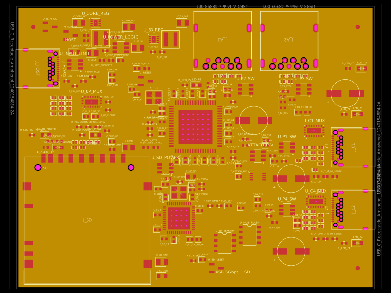 Similar packagegokul/usb3-sd-hubEngineering draft: four-layer, computer-powered USB 3 hub with one USB-C host socket, two USB-C and two USB-A accessory sockets, and a full-size SD slot. Board and three schematic previews are available. Routing and production checks are incomplete; not fabrication ready.
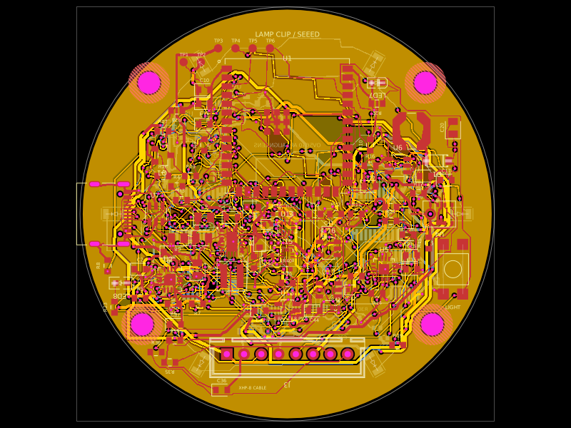 Discover something newmuse/book-reading-clip-lampA Wi‑Fi/USB‑C ESP32‑S3 reading lamp with OV5640 camera, microphone, speaker amplifier, rechargeable Li‑Po power management, six-LED boost light, USB protection/charging detection, and a clip/gooseneck enclosure with external FlexPIFA antenna.