AnasSarkiz/pedometer
A four-layer Bluetooth pedometer PCB built around a bare TI CC2340R5 MCU, 48 MHz/32.768 kHz clocks, 2.4 GHz antenna matching network, battery charger/fuel gauge, accelerometer, regulator, USB‑C, OLED/SWD connectors, and supporting passives/protection.
- Version
- 1.1.3
- License
- unset
- Stars
- 0
docs/through-via-routing.md
# Through-via routing check

The current capacity autorouter 0.0.875's `AutoroutingDrcEngine` evaluates a via on only its transition endpoint layers. On this four-layer PCB, all generated vias are physical through holes. A bottom-to-inner2 connection therefore also has copper on top and inner1.

A small regression fixture reproduces an undetected top-pad collision. The local `through-via-drc.ts` adapter expands only the repair evaluator's temporary copy to cover every routing layer. It preserves the solver's actual routes, via centers and exported transitions. No manually specified via locations are introduced. This scoring workaround does not guarantee that the repair solver will find a legal route; the final CAD and manufacturing checks remain the acceptance gates.

Physical inner1 is reserved for ground; top, inner2 and bottom form the routing stack. The independent fabrication audit also checks drills against copper on all physical layers.

Run `bun test tests/through-via-drc.test.ts` for the collision regression. This is a local workaround, not a published upstream framework fix.
Related Packages
 More from this authorAnasSarkiz/am625sip-linuxAn electronic component representing an AM625 system-in-package with mapped pins and physical footprint for PCB integration.
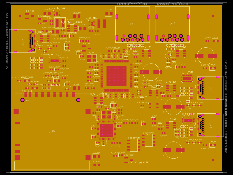 Similar packagegokul/usb3-sd-hubEngineering draft: four-layer, computer-powered USB 3 hub with one USB-C host socket, two USB-C and two USB-A accessory sockets, and a full-size SD slot. Board and three schematic previews are available. Routing and production checks are incomplete; not fabrication ready.
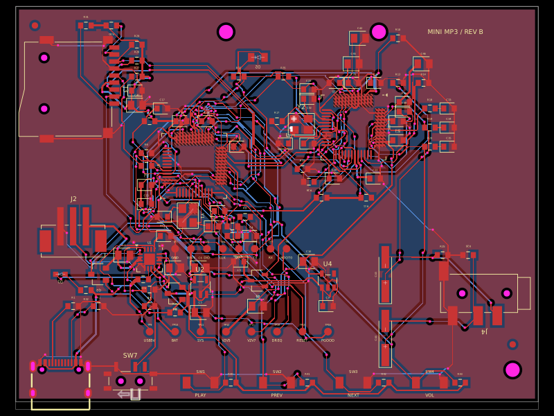 Discover something newmohan-bee/mini-mp3-playerPortable, battery-powered MP3 player hardware with USB charging, microSD storage, an MCU, VS10xx audio decoder, headphone output, status controls, and regulated power rails.