AnasSarkiz/magnetic-shutter-remote-r8
A USB‑C rechargeable battery-powered ESP32‑C3 wireless controller with Li‑ion charging, protected 3.3‑V buck‑boost regulation, thermal/safety monitoring, status LEDs, buttons, programming UART, crystal clock, and 2.4‑GHz antenna matching network.
- Version
- 0.4.0-prototype
- License
- unset
- Stars
- 0
evidence/R9-routing-2026-10-13/USB-SLOT-REVIEW.md
# USB shell-slot drawing and CAM correction — 2026-10-14

The first independent final CAM readback correctly rejected the supplier import's four plated slots. JLCPCB's published two-layer capability requires width >=0.5mm and total slot length >=2×width. The imported0.7999984mm-wide slots had total lengths1.1999976/1.499997mm and failed. Do not waive this manufacturing rule.

The retained exact HRO TYPE-C-31-M-12 drawing (`references/R9-routing/C165948.pdf`,2020-12-08,page1) specifies four0.60mm-wide plated slots,1.40mm long toward the connector mouth and1.70mm at the rear. Their center rows are4.18mm apart and center columns8.65mm apart. The supplied library's0.8×1.2/1.5 holes differ from this drawing; this is a supplier-library/drawing mismatch, not an established importer transformation bug.

`src/r9-usb-footprint.tsx` explicitly authors the drawing's0.6×1.4/1.7 holes. Original imports remain unchanged. Every electrical terminal label/center and SMT/body primitive is retained. Pin14 paste is recentered to the exact eight-vertex copper polygon:the supplier aperture was displaced0.0002032mm (0.2032µm), exceeding the retained0.0001mm attribution criterion. No checker tolerance is relaxed; other paste polygons are retained. The original1.2mm copper width is retained; the rear copper length grows2.0→2.1mm to preserve0.20mm nominal end annulus. Front1.8mm copper length remains. Slot ratios are2.333/2.833. No fitting hole is made smaller than the manufacturer's drawing. Current center errors remain below the drawing's±0.05mm layout tolerance.

The board and supplier contact-registration fixture remain distinct: assembly registration uses the unchanged independent supplier terminal centers and identifiers. This does not certify supplier hole dimensions. Actual native/copper/net/clearance/CAM checks must pass after the source change; no generated Circuit JSON or Gerber is edited.

Supplier filled/capped-via processing/cost and physical assembly qualification remain separate release gates. No supplier contact, order or upload was performed.
Related Packages
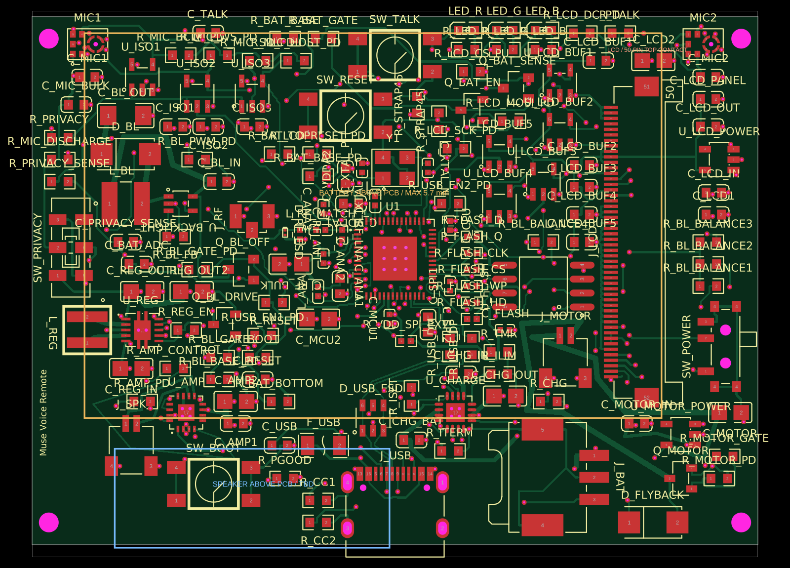 More from this authorAnasSarkiz/muse-voice-remoteMuse Voice Remote v1.3.0: checked prototype PCB/PCBA handoff. Bare ESP32-S3R8 chip, 155 TOP parts from 56 stocked JLCPCB imports with supplier CAD retained. Exact ER-TFT028A2-4 no-touch LCD, dual microphones, TALK, physical privacy, Wi-Fi, speaker, haptic and USB-C. Includes circuit.json, Gerbers/drills, JLC BOM/CPL, segmented stencil artwork and 19 filled/capped thermal-hole map. Native/factory DRC clean; 20 tests pass. See manufacturing/FABRICATION-NOTES.md for stackup and assembly requirements. Physical device/enclosure/RF qualification, firmware and connected-service MUSE integration remain unverified.
 Similar packageaura/diy-power-delivery-triggerThis hardware design implements a USB Type-C port with supporting power management and signal conditioning components, including a USB-C connector, a FUSB302 USB-C port controller, ESD protection diodes, a buck converter for 3.3V power regulation, an STM32 microcontroller for control and processing, an RGB LED indicator, push button, terminal block connections, and associated filtering and support components.
 Discover something newseveibar/am3352-ram-dogbone-and-single-layer-route-testAM3352BZCZ100 processor connected to a W631GG6MB-12 DDR3 memory chip through a routed, length-matched 16-bit DDR interface with clock/data-strobe pairs and control/address signals.