AnasSarkiz/magnetic-shutter-remote-r8
A USB‑C rechargeable battery-powered ESP32‑C3 wireless controller with Li‑ion charging, protected 3.3‑V buck‑boost regulation, thermal/safety monitoring, status LEDs, buttons, programming UART, crystal clock, and 2.4‑GHz antenna matching network.
- Version
- 0.4.0-prototype
- License
- unset
- Stars
- 0
evidence/R9-routing-2026-10-13/DATASHEET-REVIEW.md
# R9 datasheet decisions and prototype gates

This is engineering review of the selected bare-chip candidate, not measured
hardware performance. All33 purchased identities map to retained manufacturer
PDFs in `references/R9-routing/manifest.json` (24 distinct documents; resistor
and capacitor families are shared). PDFs were obtained from the public JLCPCB
listing's normal download or already retained official manufacturer documents;
expiring signed download addresses and listing HTML are not published.

| Circuit | Datasheet requirements and decisions | Routing/verification requirement |
|---|---|---|
| ESP32-C3FH4/C2858491 | Espressif v2.4 §§2,3,5: QFN32+EP,4MB in-package flash;3.0–3.6V supply. Six external supply pins2/3/11/17/31/32;33GND.18VDD_SPI is flash supply output;19–24 reserved for in-package flash. Boot GPIO2/GPIO8 high;GPIO9 low for UART download. EN10k/1uF nominal10ms. | All33 lands present; supported3.8×3.8mm EP has an explicit3.04×3.04mm paste aperture,64% coverage. Four capped through vias provide its bottom return. Pin/net audit independently covers external power, isolated flash rail, unused pins, boot/reset and UART. Top power/RF/clock, continuous bottom ground under chip/clock/RF; short local decoupling and exposed-pad return. No reuse of module routes. |
| Clock Y1/C284176 | Exact TXM40M0004252HBCEO00T:40MHz fundamental,15pF load,±10ppm initial,±30ppm temperature,±5ppm/year aging,25Ω maximum ESR,100uW drive rating;2.5×2×0.65mm. Espressif recommends±10ppm measured offset and initial24nH series XTAL_P.27pF pair assumes1.5pF stray. | No clock vias; crystal ≥2mm from chip body; local load/case grounds and bottom plane. Initial tolerance does not guarantee total temperature offset: physical frequency/drive/startup qualification remains pending. |
| Crystal land comparison | Manufacturer recommended1×0.9mm lands,centres±0.85/±0.65. Original supported import1.2×1.1mm,centres±0.95/±0.75006; recommended lands entirely contained, inner gaps retained and outer toe enlarged≈0.2mm. Terminal geometry is covered. | Engineering prototype variation accepted after physical pad/courtyard/drill audit; unchanged importer definition. No claim of exact recommended-land equality. New native crystal replaces C9010 candidate; old evidence remains retained. |
| RF L2/L4/C6980360 | Murata LQG15HN2N0B02D:2nH±0.1nH,900mA,0.09Ω maximum DC resistance,6GHz minimum self-resonance. L2 filters RF supply; L4 is an initial2–3nH-range chip matching value. One shared purchased identity avoids an additional assembly setup. | Short power loop for L2; L4 between chip and antenna feed. RF performance/harmonics must be physically tuned in final enclosure. |
| RF C21/C22/C76900 | GJM1555C1H1R5BB01D:1.5pF±0.1pF,C0G,50V,high-Q0402. Espressif initial shunt range1.2–1.8pF; guide explicitly says harmonic stub is not required with0402 and above. | Replaces0201 candidate, permits a two-layer reference and larger process spacing. Keep short ground returns; no RF signal vias. Values are starting values, not tuned results. |
| ANT1/C22423581 | Pulse ANT3216LL00R2400A,3.2±0.15×1.6±0.15×1.2±0.15mm,terminal length0.4±0.2mm. Pin1RF; support pin2unconnected. Manufacturer drawing shows an evaluation-board feed/support geometry, not a stated mandatory land tolerance for every host board. | Imported1×1.750009mm pads at±1.578102 cover nominal terminal widths and contain recommended feed land. Reference support-tail/ground/host differences remain RF tuning inputs, not proof of an open circuit. All-layer clear antenna region; move to upper-right away from battery foil/MagSafe array; verify actual new model and metal spacing. No universal RF/phone compatibility claim. |
| BQ25185/C19725033 | TI current §7:IN3.3–18V;IN/BAT/SYS close bypass,ground/EP plane. R3=1k nominal300mA,tolerance267.3–333.3mA. R8=130k selects4.1V/500mA-input mode;4.1205V upper target. Fixed10kTS permitted with separate temperature guard. | Short/wide IN,BAT,SYS loops,thermal ground; preserve independent charge-disable gate. USB input turns radio off. Recalculate actual routed drops and inspect bypass distance, not just source membership. |
| TPS63031/C15516 + L1/C56594 | TI fixed3.3V buck-boost;VIN5/VINA8 battery,FB10/VOUT1 output,EN6,PS7ground,GND9/PGND3/EP11ground;L1 between pins4/2. SWPA3015S1R5NT is1.5uH±30%,minimum1.05uH,2.3A saturation/1.7A RMS. TI layout requires short wide power loops,local input/output/VINA bypass and control/power ground meeting near IC. | Retain switch-node segregation, audited±30% worst-case peak/RMS and20% saturation headroom.500mA output budget and battery input ≤1A; routed neck widths/drop must pass fresh R9 audit. Capacitor DC-bias load-step response remains physical qualification. |
| U4/C485802,SW1/C431540,Q1/Q2/C8545 | TPS3839G33 cutoff3.003–3.126V;31mV typical hysteresis;120–350ms release. SPDT ON accepts cutoff signal;OFF grounds regulator EN.2N7002 gate/source/drain maps audited;USB disables radio;temperature-good permits charge. | Correct physical drain/source/gate mapping and isolated nets, steady OFF low and no charge-disable leakage assumption without testing. |
| TMP390A2/C5219772,R10/R11 | TI tables7-1/7-2:R10=1.62k selects nominal36°C hot,R11=18.7k selects5°C cold/5°C hysteresis. Conservative thresholds remain inside selected cell0–50°C range, subject to sensor tolerance and thermal gradient; original resistor identities retained. | Correct polarity/threshold nets; effective thermal coupling to actual cell required. PCB sensor alone is not a certified battery temperature measurement. |
| J1/C165948 | HRO TYPE-C-31-M-12 charge-only sink:all four shell contacts and both GND lands ground,both VBUS lands5V,CC1/CC2 separate5.1k pulls;DP/DN/SBU unused. | Native standard USB-C schematic; actual supplier alias→pad→net map verified;original paste polygons preserved by canonical core fix105. Copper-to-edge/NPTH/PTH/pad tests pass unrouted. New shell/CAD mouth must be checked against enclosure opening. |
| J2/C160402,J3/C160389 | Exact JST SH battery header mates SHR-02V-S-B pack;BM03B-SRSS-TB top-entry programmer header carries only RX/GND/TX. Standard programmer0.8.0J5:TX→board contact1RX(GPIO20),GND2,contact3TX(GPIO21)→programmer RX. Fixed3.3V signalling;no power/BOOT/EN pins. | Battery powers target;manual BOOT+RESET required. Preserve correct cable mating/orientation. Missing3V3 metadata remains a separate importer issue. Physical cable/flash/enumeration untested. Native J3 orientation warning is inherited issue004: the actual top-entry socket is accessed with the lid off, not from a PCB edge; no generated metadata edit or warning suppression. |
| Buttons/LED/passives | TS24CA/C393942 right-edge shutter50mA12V,travel0.15±0.05mm,160±50gf,20k mechanical operations. Other momentary/slide switches and LED polarity/rating read from retained family drawings.0603WAF resistor codes:0.1W,±1%. RF/crystal C0G and power X7R/X5R values/rated voltages checked from exact family codes. | Shutter pose unchanged;lid-off BOOT/RESET/pair access. Recheck every actual CAD model/courtyard and preserve same-page component explanations. High-value MLCC DC-bias curves are not guaranteed by nominal BOM values. |
| External battery | TinyCircuits ASR00012/Hondark803040PL-1000mAh protected1S:maximum32×43×8.5mm,4.2V maximum charge,500mA standard/1A maximum charge,1A maximum discharge,0–50°C charge. |300mA/4.1V charge below limits. Budget peak input and connector limits;verify battery clearance,lead strain relief,insulation,thermal coupling and swell allowance with actual pack. No claimed JLC ID for external cell. |

Issue104's antenna reference-layout concern is narrowed to physical RF/process
qualification; reference geometry differences alone do not establish fabrication
impossibility. This acceptance covers an engineering prototype only. Native and
independent DRC, routing, Gerber/paste/drill, model fit and actual supplier mapping
must still pass independently before claiming first-prototype fabrication ready.
Related Packages
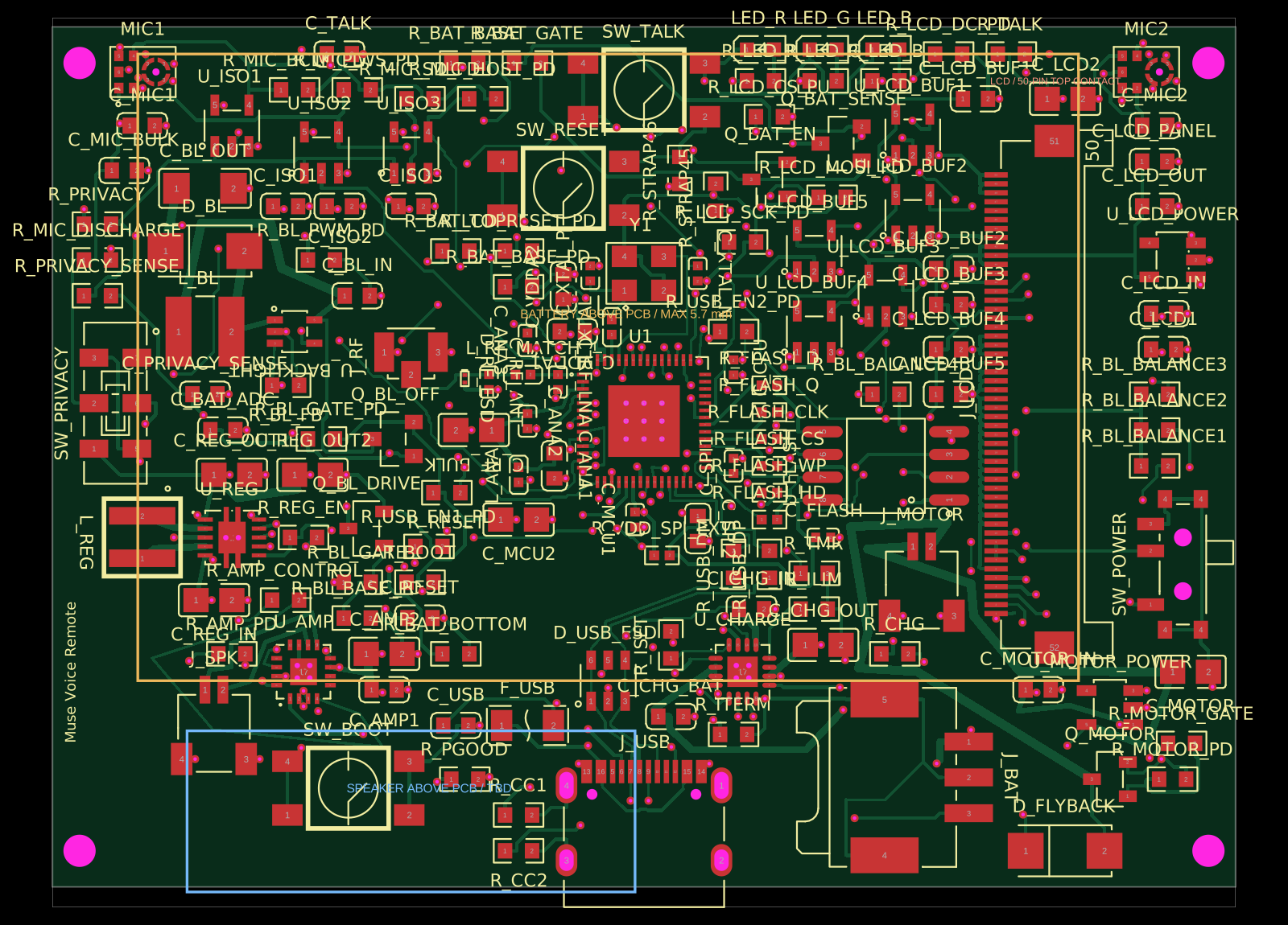 More from this authorAnasSarkiz/muse-voice-remoteMuse Voice Remote v1.3.0: checked prototype PCB/PCBA handoff. Bare ESP32-S3R8 chip, 155 TOP parts from 56 stocked JLCPCB imports with supplier CAD retained. Exact ER-TFT028A2-4 no-touch LCD, dual microphones, TALK, physical privacy, Wi-Fi, speaker, haptic and USB-C. Includes circuit.json, Gerbers/drills, JLC BOM/CPL, segmented stencil artwork and 19 filled/capped thermal-hole map. Native/factory DRC clean; 20 tests pass. See manufacturing/FABRICATION-NOTES.md for stackup and assembly requirements. Physical device/enclosure/RF qualification, firmware and connected-service MUSE integration remain unverified.
 Similar packageaura/diy-power-delivery-triggerThis hardware design implements a USB Type-C port with supporting power management and signal conditioning components, including a USB-C connector, a FUSB302 USB-C port controller, ESD protection diodes, a buck converter for 3.3V power regulation, an STM32 microcontroller for control and processing, an RGB LED indicator, push button, terminal block connections, and associated filtering and support components.
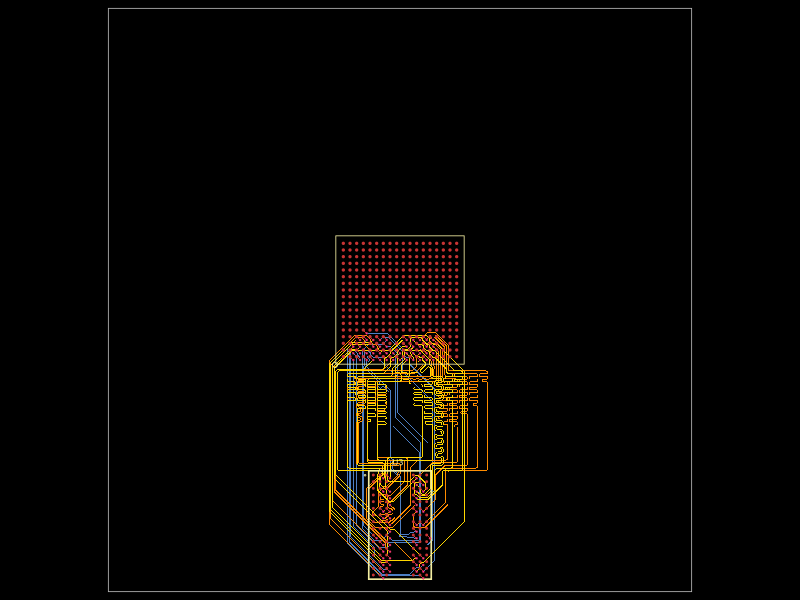 Discover something newseveibar/am3352-ram-dogbone-and-single-layer-route-testAM3352BZCZ100 processor connected to a W631GG6MB-12 DDR3 memory chip through a routed, length-matched 16-bit DDR interface with clock/data-strobe pairs and control/address signals.