0hmX/esp32-s3-usb-webcam-ov2640
This code defines and integrates a variety of surface-mount, through-hole, and connector hardware components (including microcontrollers, regulators, resistors, capacitors, and connectors) into a PCB design framework, enabling schematic symbol creation, footprint definition, and automated routing within an electronic circuit layout.
- Version
- 1.0.7
- License
- unset
- Stars
- 0
tests/manual-fanout-output.test.ts
import { expect, test } from "bun:test"
import {
  BOARD_ROUTING_PHASES,
  assertBoardRoutingPhaseSelectorsAreUnique,
} from "../src/routing-phases"
import { postprocessEspEnVia } from "../src/esp-en-via-postprocess-autorouter"

type CircuitElement = Record<string, any>

const circuit = (await Bun.file("dist/index/circuit.json").json()) as CircuitElement[]

test("board and top-only assembly invariants are preserved", () => {
  const board = circuit.find((element) => element.type === "pcb_board")
  expect(board).toMatchObject({ width: 65.5, height: 42.5, num_layers: 4 })

  const components = circuit.filter((element) => element.type === "pcb_component")
  expect(components.length).toBeGreaterThan(0)
  expect(components.every((component) => component.layer === "top")).toBe(true)

  const mountingHoles = circuit.filter(
    (element) =>
      element.type === "pcb_hole" &&
      element.pcb_component_id === null &&
      element.hole_diameter === 2.7,
  )
  expect(mountingHoles).toHaveLength(4)
  expect(circuit.filter((element) => element.type === "pcb_keepout")).toHaveLength(5)
})

test("manual FPC fanout and remapped camera routing are complete", () => {
  const byName = new Map(
    circuit
      .filter((element) => element.type === "source_component")
      .map((component) => [component.name, component]),
  )
  expect(byName.get("J_CAM")?.manufacturer_part_number).toBe("AFC01-S24FCA-00")

  const fanoutSource = byName.get("CAM_FANOUT_VIAS")
  const fanoutPcb = circuit.find(
    (element) =>
      element.type === "pcb_component" &&
      element.source_component_id === fanoutSource?.source_component_id,
  )
  expect(fanoutPcb?.do_not_place).toBe(true)

  const namedFanoutTraces = circuit.filter(
    (element) =>
      element.type === "source_trace" && element.name?.startsWith("TRACE_CAM_"),
  )
  expect(namedFanoutTraces).toHaveLength(39)
  expect(
    circuit.filter((element) => element.type === "pcb_port_not_connected_error"),
  ).toHaveLength(0)
})

test("routing phase selectors remain unique", () => {
  const selectors = assertBoardRoutingPhaseSelectorsAreUnique()
  expect(selectors.size).toBe(45)
  expect(BOARD_ROUTING_PHASES).toHaveLength(4)
})

test("compact proven-route artifact is fully routed and error-free", () => {
  const errors = circuit.filter((element) => element.type.endsWith("_error"))
  expect(errors).toHaveLength(0)
  expect(circuit.filter((element) => element.type === "pcb_trace")).toHaveLength(
    149,
  )
  expect(circuit.filter((element) => element.type === "pcb_via")).toHaveLength(
    151,
  )

  const routeContains = (
    trace: CircuitElement,
    x: number,
    y: number,
    routeType?: string,
  ) =>
    trace.route?.some(
      (point: CircuitElement) =>
        Math.abs(point.x - x) < 0.001 &&
        Math.abs(point.y - y) < 0.001 &&
        (!routeType || point.route_type === routeType),
    )
  const traces = circuit.filter((element) => element.type === "pcb_trace")

  const dnDuplicateJoin = traces.find(
    (trace) =>
      routeContains(trace, -26.1259568, 0.250064) &&
      routeContains(trace, -26.1259568, 1.250062),
  )
  expect(
    dnDuplicateJoin?.route.filter(
      (point: CircuitElement) => point.route_type === "via",
    ),
  ).toHaveLength(2)
  expect(
    dnDuplicateJoin?.route.some(
      (point: CircuitElement) =>
        point.route_type === "wire" && point.layer === "bottom",
    ),
  ).toBe(true)

  const usbGroundEscape = traces.find((trace) =>
    routeContains(trace, -26.1258552, -2.7000063),
  )
  expect(routeContains(usbGroundEscape ?? {}, -25.1008692, -3.5, "via")).toBe(
    true,
  )

  const pwdnGroundEscape = traces.find((trace) =>
    routeContains(trace, -5.5, -9.175),
  )
  expect(routeContains(pwdnGroundEscape ?? {}, -4.25, -9.175, "via")).toBe(
    true,
  )
})

test("ESP32 EPAD uses four grounded gap vias and no via-in-pad", () => {
  const u1Source = circuit.find(
    (element) =>
      element.type === "source_component" && element.name === "U1",
  )
  const u1Pcb = circuit.find(
    (element) =>
      element.type === "pcb_component" &&
      element.source_component_id === u1Source?.source_component_id,
  )
  const pin41SourcePortIds = new Set(
    circuit
      .filter(
        (element) =>
          element.type === "source_port" &&
          element.source_component_id === u1Source?.source_component_id &&
          element.port_hints?.includes("pin41"),
      )
      .map((port) => port.source_port_id),
  )
  const pin41PcbPortIds = new Set(
    circuit
      .filter(
        (element) =>
          element.type === "pcb_port" &&
          pin41SourcePortIds.has(element.source_port_id),
      )
      .map((port) => port.pcb_port_id),
  )
  const epadLands = circuit.filter(
    (element) =>
      element.type === "pcb_smtpad" &&
      element.pcb_component_id === u1Pcb?.pcb_component_id &&
      pin41PcbPortIds.has(element.pcb_port_id),
  )
  expect(epadLands).toHaveLength(9)

  const expectedViaCenters = [
    [2.799852, 5.8748527],
    [4.1999, 5.8748527],
    [2.799852, 7.2749007],
    [4.1999, 7.2749007],
  ]
  const gapVias = circuit.filter(
    (element) =>
      element.type === "pcb_via" &&
      expectedViaCenters.some(
        ([x, y]) =>
          Math.abs(element.x - x) < 1e-6 && Math.abs(element.y - y) < 1e-6,
      ),
  )
  expect(gapVias).toHaveLength(4)

  const gnd = circuit.find(
    (element) => element.type === "source_net" && element.name === "GND",
  )
  const epadPour = circuit.find(
    (element) =>
      element.type === "pcb_copper_pour" &&
      element.layer === "top" &&
      element.source_net_id === gnd?.source_net_id &&
      element.covered_with_solder_mask === true,
  )
  expect(epadPour).toBeDefined()
  const pourVertices = epadPour?.brep_shape.outer_ring.vertices ?? []
  const pourBounds = {
    minX: Math.min(...pourVertices.map((point: any) => point.x)),
    maxX: Math.max(...pourVertices.map((point: any) => point.x)),
    minY: Math.min(...pourVertices.map((point: any) => point.y)),
    maxY: Math.max(...pourVertices.map((point: any) => point.y)),
  }
  for (const pad of epadLands) {
    expect(pad.x >= pourBounds.minX && pad.x <= pourBounds.maxX).toBe(true)
    expect(pad.y >= pourBounds.minY && pad.y <= pourBounds.maxY).toBe(true)
  }

  for (const via of gapVias) {
    expect(via).toMatchObject({
      source_net_id: gnd?.source_net_id,
      hole_diameter: 0.2,
      outer_diameter: 0.45,
      from_layer: "top",
      to_layer: "bottom",
    })
    expect(via.x >= pourBounds.minX && via.x <= pourBounds.maxX).toBe(true)
    expect(via.y >= pourBounds.minY && via.y <= pourBounds.maxY).toBe(true)

    for (const pad of epadLands) {
      const dx = Math.max(Math.abs(via.x - pad.x) - pad.width / 2, 0)
      const dy = Math.max(Math.abs(via.y - pad.y) - pad.height / 2, 0)
      expect(Math.hypot(dx, dy)).toBeGreaterThan(via.outer_diameter / 2)
    }
  }
})

test("ESP_EN postprocessor changes only the colliding transition", () => {
  const input = {
    layerCount: 4,
    minTraceWidth: 0.1,
    bounds: { minX: -10, maxX: 10, minY: -10, maxY: 12 },
    obstacles: [
      {
        type: "rect",
        layers: ["top", "inner1", "inner2", "bottom"],
        center: { x: 0, y: 10 },
        width: 10,
        height: 2,
        connectedTo: [],
      },
    ],
    connections: [
      {
        name: "source_net_13",
        pointsToConnect: [
          { x: -1, y: 0, layer: "top" },
          { x: 1, y: 0, layer: "top" },
        ],
      },
    ],
  } as any
  const traces = [
    {
      type: "pcb_trace",
      pcb_trace_id: "esp-en",
      connection_name: "source_net_13",
      route: [
        { route_type: "wire", x: 0, y: 8.9, width: 0.15, layer: "top" },
        {
          route_type: "via",
          x: 0,
          y: 8.9,
          from_layer: "bottom",
          to_layer: "top",
          via_diameter: 0.4,
          via_hole_diameter: 0.2,
        },
        {
          route_type: "wire",
          x: 0,
          y: 8.9,
          width: 0.15,
          layer: "bottom",
        },
        {
          route_type: "wire",
          x: 0,
          y: 7,
          width: 0.15,
          layer: "bottom",
        },
      ],
    },
    {
      type: "pcb_trace",
      pcb_trace_id: "unchanged",
      connection_name: "source_net_1",
      route: [
        { route_type: "wire", x: -5, y: -5, width: 0.15, layer: "top" },
        { route_type: "wire", x: 5, y: -5, width: 0.15, layer: "top" },
      ],
    },
  ] as any

  const result = postprocessEspEnVia(input, traces, { x: 0.4, y: -0.3 })
  expect(result[1]).toBe(traces[1])
  expect(result[0].route.slice(0, 3)).toEqual([
    { route_type: "wire", x: 0.4, y: 8.6, width: 0.15, layer: "top" },
    {
      route_type: "via",
      x: 0.4,
      y: 8.6,
      from_layer: "bottom",
      to_layer: "top",
      via_diameter: 0.4,
      via_hole_diameter: 0.2,
    },
    {
      route_type: "wire",
      x: 0.4,
      y: 8.6,
      width: 0.15,
      layer: "bottom",
    },
  ])
  expect(result[0].route[3]).toBe(traces[0].route[3])
})

test("ESP_EN postprocessor is a no-op when the router avoids the keepout", () => {
  const input = {
    layerCount: 4,
    minTraceWidth: 0.1,
    bounds: { minX: -10, maxX: 10, minY: -10, maxY: 12 },
    obstacles: [
      {
        type: "rect",
        layers: ["top", "inner1", "inner2", "bottom"],
        center: { x: 0, y: 10 },
        width: 10,
        height: 2,
        connectedTo: [],
      },
    ],
    connections: [
      {
        name: "source_net_13",
        pointsToConnect: [
          { x: -1, y: 0, layer: "top" },
          { x: 1, y: 0, layer: "top" },
        ],
      },
    ],
  } as any
  const traces = [
    {
      type: "pcb_trace",
      pcb_trace_id: "esp-en-clear",
      connection_name: "source_net_13",
      route: [
        { route_type: "wire", x: 0, y: 7, width: 0.15, layer: "top" },
        { route_type: "wire", x: 2, y: 7, width: 0.15, layer: "top" },
      ],
    },
  ] as any

  expect(postprocessEspEnVia(input, traces, { x: 0.4, y: -0.3 })).toBe(
    traces,
  )
})
Related Packages
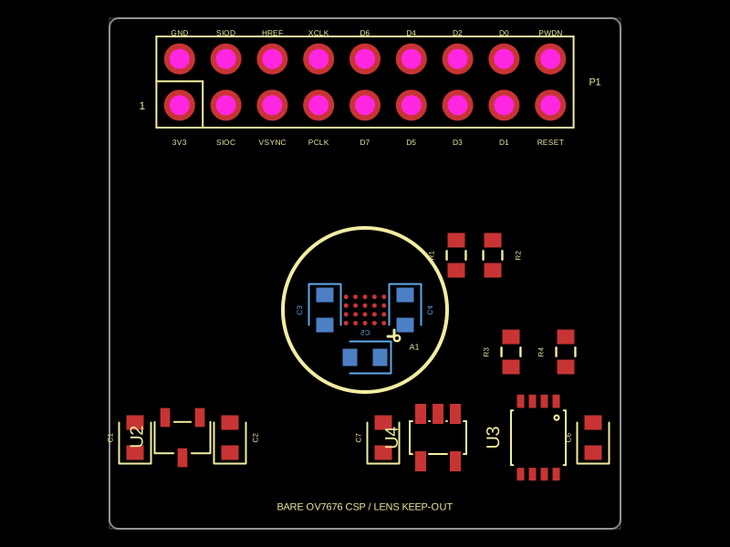 More from this author0hmX/ov7670-camera-moduleThis code defines the hardware layout and schematic connectivity for an OV7676 camera module featuring a CSP5 sensor package, power regulation, and interface connectors.
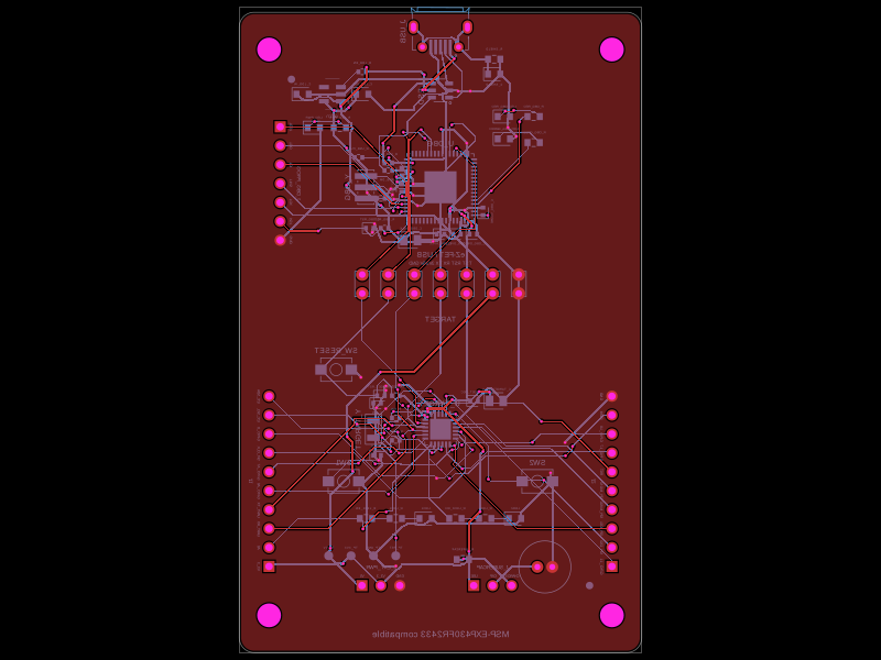 Similar packageShiboSoftwareDev/i-wanThis code defines a PCB and schematic for a microcontroller development board, incorporating various surface-mount components (resistors, capacitors, headers, connectors, crystals, and an IC), with detailed footprints, electrical nets, and routing instructions.
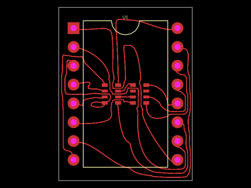 Discover something newseveibar/single-layer-tdA single-chip DIP-16 package circuit connecting pins 1–8 to corresponding internal pins 9–16.