0hmX/esp32-s3-usb-webcam-ov2640
This code defines and integrates a variety of surface-mount, through-hole, and connector hardware components (including microcontrollers, regulators, resistors, capacitors, and connectors) into a PCB design framework, enabling schematic symbol creation, footprint definition, and automated routing within an electronic circuit layout.
- Version
- 1.0.7
- License
- unset
- Stars
- 0
imports/TLV62569DBVR.tsx
import type { ChipProps } from "@tscircuit/props"

const pinLabels = {
  pin1: ["EN"],
  pin2: ["GND"],
  pin3: ["SW"],
  pin4: ["VIN"],
  pin5: ["FB"]
} as const

const pinAttributes = {
  pin2: {requiresGround: true},
  pin4: {requiresPower: true}
} as const

export const TLV62569DBVR = (props: ChipProps<typeof pinLabels>) => {
  return (
    <chip
      pinLabels={pinLabels}
      pinAttributes={pinAttributes}
      supplierPartNumbers={{
  "jlcpcb": [
    "C141836"
  ]
}}
      manufacturerPartNumber="TLV62569DBVR"
      footprint={<footprint>
        <smtpad portHints={["pin5"]} pcbX="-1.300099mm" pcbY="-0.94996mm" width="1.0999978mm" height="0.5999988mm" shape="rect" />
<smtpad portHints={["pin4"]} pcbX="-1.300099mm" pcbY="0.94996mm" width="1.0999978mm" height="0.5999988mm" shape="rect" />
<smtpad portHints={["pin3"]} pcbX="1.300099mm" pcbY="0.94996mm" width="1.0999978mm" height="0.5999988mm" shape="rect" />
<smtpad portHints={["pin2"]} pcbX="1.300099mm" pcbY="-0mm" width="1.0999978mm" height="0.5999988mm" shape="rect" />
<smtpad portHints={["pin1"]} pcbX="1.300099mm" pcbY="-0.94996mm" width="1.0999978mm" height="0.5999988mm" shape="rect" />
<silkscreenpath route={[{"x":0.8999728000000005,"y":-1.404111999999941},{"x":0.8999728000000005,"y":-1.5500604000000067}]} />
<silkscreenpath route={[{"x":0.8999728000000005,"y":-0.45412660000010874},{"x":0.8999728000000005,"y":-0.4958079999998972}]} />
<silkscreenpath route={[{"x":0.8999728000000005,"y":0.4958079999998972},{"x":0.8999728000000005,"y":0.45415200000002187}]} />
<silkscreenpath route={[{"x":0.8999728000000005,"y":1.5499587999998994},{"x":0.8999728000000005,"y":1.404111999999941}]} />
<silkscreenpath route={[{"x":-0.9000489999999672,"y":-1.404111999999941},{"x":-0.9000489999999672,"y":-1.5500604000000067}]} />
<silkscreenpath route={[{"x":-0.9000489999999672,"y":0.4958079999998972},{"x":-0.9000489999999672,"y":-0.4958334000000377}]} />
<silkscreenpath route={[{"x":-0.9000489999999672,"y":1.5499587999998994},{"x":-0.9000489999999672,"y":1.4040866000000278}]} />
<silkscreenpath route={[{"x":-0.9000489999999672,"y":1.5499587999998994},{"x":0.8999728000000005,"y":1.5499587999998994}]} />
<silkscreenpath route={[{"x":-0.9000489999999672,"y":-1.5500604000000067},{"x":0.8999728000000005,"y":-1.5500604000000067}]} />
<silkscreentext text="{NAME}" pcbX="0.012319mm" pcbY="2.562354mm" anchorAlignment="center" fontSize="1mm" />
<courtyardoutline outline={[{"x":-2.091880999999944,"y":1.8123540000000276},{"x":2.1165190000000393,"y":1.8123540000000276},{"x":2.1165190000000393,"y":-1.786446000000069},{"x":-2.091880999999944,"y":-1.786446000000069},{"x":-2.091880999999944,"y":1.8123540000000276}]} />
      </footprint>}
      cadModel={{
        objUrl: "https://modelcdn.tscircuit.com/easyeda_models/assets/C141836.obj?uuid=460193f9bf2d42e58cf3c2f675b07dc6",
        stepUrl: "https://modelcdn.tscircuit.com/easyeda_models/assets/C141836.step?uuid=460193f9bf2d42e58cf3c2f675b07dc6",
        pcbRotationOffset: 180,
        modelOriginPosition: { x: 0, y: -0.000012700000070253736, z: -0.049083 },
      }}
      {...props}
    />
  )
}
Related Packages
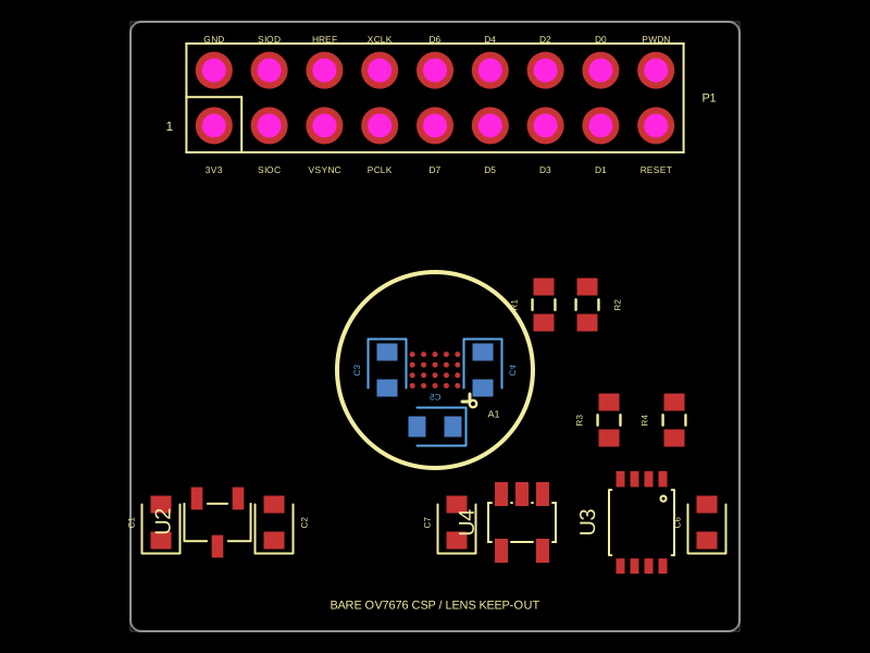 More from this author0hmX/ov7670-camera-moduleThis code defines the hardware layout and schematic connectivity for an OV7676 camera module featuring a CSP5 sensor package, power regulation, and interface connectors.
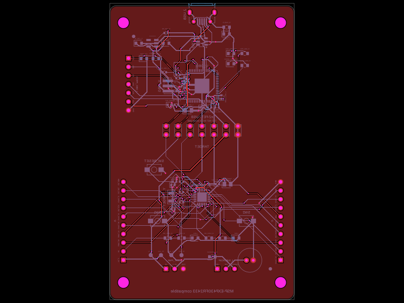 Similar packageShiboSoftwareDev/i-wanThis code defines a PCB and schematic for a microcontroller development board, incorporating various surface-mount components (resistors, capacitors, headers, connectors, crystals, and an IC), with detailed footprints, electrical nets, and routing instructions.
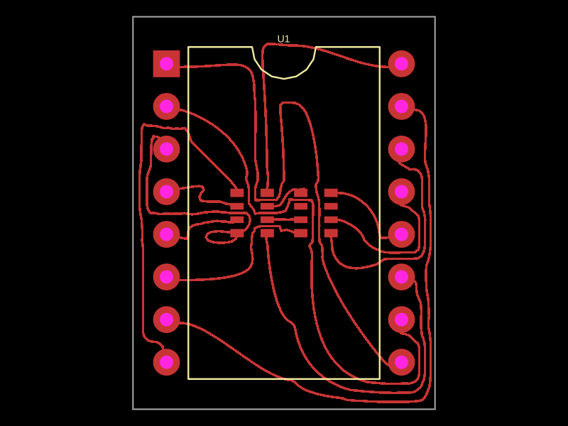 Discover something newseveibar/single-layer-tdA single-chip DIP-16 package circuit connecting pins 1–8 to corresponding internal pins 9–16.