0hmX/dual-usb-peltier-assembly
A tscircuit package created by 0hmX.
- Version
- 0.4.12
- License
- unset
- Stars
- 0
docs/pcb-fabrication.md
# PCB fabrication and routing basis

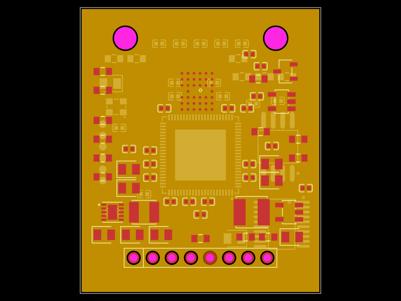
Design basis recorded 2026-10-17. The 72.5 × 59 mm board uses top-side assembly, four layers, a nominal 1.6 mm finished thickness, 2 oz outer copper and 1 oz inner copper. Specify **JLC041621-7628** when ordering; substituting another 1.6 mm stack changes the USB impedance.

| Layer or dielectric | Vendor thickness | Function / dielectric constant |
| --- | ---: | --- |
| L1, top copper | 0.070 mm | Components and broad power copper |
| 7628 prepreg | 0.203 mm | Er 4.4 |
| L2, inner1 copper | 0.030 mm | Whole-board ground return |
| Core | 1.030 mm | Er 4.6 |
| L3, inner2 copper | 0.030 mm | Ground beneath USB; local power and signal escapes elsewhere |
| 7628 prepreg | 0.203 mm | Er 4.4 |
| L4, bottom copper | 0.070 mm | Signals and local copper |

These are the [JLCPCB stackup selector](https://jlcpcb.com/impedance) values for template code `20220617083632`; its compressed total is 1.636 mm. The vendor labels the inner copper 1 oz but specifies 0.030 mm, which is the thickness used below. The [copper-weight guide](https://jlcpcb.com/help/article/jlcpcb-copper-weight) documents the available copper weights.

## Manufacturing rules

The board source sets 0.20 mm minimum trace width; 0.17 mm trace-to-pad, pad-to-pad and via-edge-to-pad clearance; 0.30 mm via drills with 0.60 mm pads; 0.25 mm trace-to-hole and hole-to-hole clearance; and 0.30 mm copper-to-board-edge clearance. Non-POFV via drills must also remain at least 0.15 mm from SMT solder lands, including same-net lands; this separate fabrication margin is checked in the routing tests. Use at least 0.20 mm copper clearance where placement permits. Local bounded pours use `boardEdgeMargin={0}` to retain their specified outer outline; their clearances to other copper and the actual board boundary still require checking in the exported geometry. Fine-pitch package lands follow their footprints and require the selected 2 oz process to pass fabrication review. JLC's [2 oz guidance](https://jlcpcb.com/help/article/jlcpcb-copper-weight) lists 0.16 mm minimum trace/space.

Intentional same-net thermal vias intersecting exposed solder lands, including the MCU and PD controller ground arrays, require **epoxy fill, planarization and copper caps (POFV)**. Apply this treatment to any converter thermal vias that intersect solder lands in the final layout. The 0.30 mm drill is within JLC's published 0.20–0.50 mm POFV range; [POFV is available for four-layer boards as a charged process](https://jlcpcb.com/news/free-via-in-pad-6-20-layer-pcbs-pofv). Specify the affected via coordinates or all 0.30 mm vias in the order notes and confirm the production files. [JLC's via-covering rules](https://jlcpcb.com/help/article/pcb-via-covering) explicitly exclude via-in-pad from ordinary solder-mask ink plugging and support epoxy-filled, copper-capped pads. Open holes or ordinary tenting are not the release process for these arrays. Use ENIG where exposed copper spacing is below 0.20 mm, following the same vendor guidance. A DRC exception for a named same-net thermal array verifies placement intent only; it does not verify the ordered fill/cap process or authorize signal drill-in-pad.

## Power copper and returns

The routing assumptions are 5 A maximum USB input, 6 A / 72 W maximum load output, an 8 A inductor-path screening current, and 50 °C ambient. The preliminary copper screen allows 10 °C trace self-heating. Using `I = k × ΔT^0.44 × A^0.725`, with area in square mils and `k = 0.048` for outer copper or `0.024` for inner copper, gives:

| Current | 70 µm outer copper width | 30 µm inner copper width |
| ---: | ---: | ---: |
| 5 A | 1.38 mm | 8.39 mm |
| 6 A | 1.78 mm | 10.79 mm |
| 8 A | 2.64 mm | 16.05 mm |

The relationship is reproduced in [TI TIDUCS7, equation 7](https://www.ti.com/lit/pdf/tiducs7). It is an initial cross-section screen, not a measured board current rating. Main outer-layer power corridors target at least 3 mm of **remaining copper after clipping**, preferably 4 mm. Local internal power areas supplement the outer copper; they are not assigned the full 6 A through narrow inner-layer traces. Package escapes may use 0.22–0.30 mm copper for the shortest feasible distance before widening; the target is no more than 0.5 mm outside a pad or broad pour. Their thermal behavior depends on heat spreading into the lands and pours and must be checked separately.

The retained converter layout has clearance-constrained exceptions: the VIN escape uses 0.22 mm copper for approximately 0.875 mm before widening, and the final rendered VOUT path has approximately 1.14 mm of narrow copper; each SW escape has about 0.239 mm. The output HF-capacitor-to-main-copper transition reaches a minimum 1.00 mm copper span; approximately 2.71 mm of that route remains below the 1.78 mm screening width. These local transitions exceed the narrow-escape length target or fall below the uniform-trace screen. Their adjacent copper can spread heat, but they require temperature measurements at the stated load and ambient before the 6 A operating limit is validated.

The 72.5 × 59 mm outline has 46.5% less board area and reduces available ground copper. Retained converter geometry and thermal-via arrays do not establish unchanged thermal performance; qualify the compact board at the intended current, ambient and airflow.

Use ten parallel 0.30/0.60 mm vias for each VIN/VOUT power-layer bank and twelve for the converter PGND bank, with broad copper entering and leaving the bank. Ten vias would share 6 A at 0.6 A each under ideal sharing. [TI SLVA959B, table 3-1](https://www.ti.com/lit/pdf/slva959) gives 0.84 A for a 12 mil via at 10 °C rise under its stated assumptions; it supports the initial bank sizing, not a guarantee of equal sharing. The barrel basis is at least 20 µm average / 18 µm local plating from [JLCPCB's plating guide](https://jlcpcb.com/blog/mastering-pcb-plating). No full-current transition should depend on one serial via or a narrow bank entrance.

L2 is the whole-board ground plane. Each of the eight converter input/output ceramic ground lands has a three-via bank; input bulk and TEC bulk have ten each, and the main fan capacitors have three each. Solid top patches and 0.8 mm links join these lands to their banks. Inspect the complete high-current return for necks: a lone 30 µm inner-layer return needs substantially more width than the 70 µm outer power path. L3 provides ground beneath the bottom USB corridor and its connector/MCU transitions; local power islands lie outside that reference area. Selected signal escapes use L3 away from the USB projection, with at least 0.60 mm between their new ground cutouts and USB copper. Separate shunt sense branches leave opposite lands and use pour notches to exclude load current. The top-side 10 Ω / 220 nF filter sits outside the main power pours; its layer transitions and the top compensation ground keep the sense taps separate from load current. Compensation and FSW ground join at the VCC capacitor ground region. Their top-side placements use inner2 signal escapes beneath the inner1 ground plane; include switching-frequency and loop-noise measurements in the existing bench qualification. Analog ground joins the power return at the VCC capacitor ground region. These choices follow the [TPS55289 layout guidance](https://www.ti.com/lit/ds/symlink/tps55289.pdf), including short switching loops, Kelvin sensing and multiple PGND vias.

The compact board places the fan buck between the USB ports. Its 12 V / 0.5 A output uses a 88.91 mm, 0.60 mm-wide outer-layer branch through the programming-supply gap and along the bottom edge, with three 0.30/0.60 mm layer transitions. At 70 °C, the trace-only estimate is approximately 24 mV at 0.5 A (70 µm copper); the whole-board inner1 plane supplies the return. The converter input and output capacitor banks retain their original via counts. Main TEC power corridors and VIN/VOUT/PGND bank sizes remain unchanged.

## Control-supply routing

`CTRL_3V3` may use 0.20 mm dense routes and package escapes on the 70 µm outer layers, retaining 0.40 mm trunks where space permits and the existing local bypass connections. Screen each source-to-load path at 500 mA with at most **60 mm equivalent 0.20 mm length**, calculated as `L_0.20 + 0.5 × L_0.40` for outer copper; multiply any 30 µm inner-layer contribution by `70/30`. This is a path budget, not the sum of the supply tree. Assuming copper resistivity 1.724 × 10⁻⁸ Ωm at 20 °C and a 0.00393/°C coefficient, 0.20 mm copper is approximately 1.47 mΩ/mm at 70 °C: a 60 mm path drops 44 mV at 500 mA; a 5 mm escape drops 3.7 mV. Evaluate shared segments with their branch currents; vias, ground return, regulator tolerance and transients consume additional voltage margin.

The fitted logic and two selected probes have an initial 100–200 mA load allocation, subject to firmware and attached-load verification. The conservative 500 mA conductor screen uses the [TLV75533 output rating](https://www.ti.com/lit/ds/symlink/tlv755p.pdf); it does not qualify continuous board current. At 5 V input, 500 mA would dissipate about 0.85 W in the regulator. The [RP2040 USB supply minimum is 3.135 V](https://datasheets.raspberrypi.com/rp2040/rp2040-datasheet.pdf), so confirm final source-to-load drops and dynamic supply margin on hardware.

Screen the separate `RP_CORE_1V1` distribution at the RP2040 regulator's 100 mA rating. Its nominal 1.1 V output, −3% regulator corner and 1.05 V DVDD minimum leave 17 mV for distribution, return and transient losses. Target no more than 10 mV of trace and barrel drop to either DVDD pin at 100 mA. Use the actual traversed via spans and 30 µm inner copper in this calculation; the remaining static allowance does not establish transient margin. These limits follow the [RP2040 datasheet's regulator and supply specifications](https://datasheets.raspberrypi.com/rp2040/rp2040-datasheet.pdf).

The paths before the 19 October 2026 `CTRL_3V3` cleanup give the following conservative conductor-drop bounds at 70 °C copper temperature, including the traversed barrel spans with 18 µm plating. The cleanup shortens branches and removes staircase bends while retaining widths, vias, supply junctions and local bypass connections. Each destination is screened independently at the total rail current; these are not simultaneous per-pin current assignments.

| Source-to-load path | Screening current | Trace and barrel drop |
| --- | ---: | ---: |
| 3.3 V regulator to USB_VDD | 500 mA | 22.82 mV |
| Worst MCU 3.3 V destination | 500 mA | 47.28 mV |
| RP2040 regulator to DVDD23 | 100 mA | 5.90 mV |
| RP2040 regulator to DVDD50 | 100 mA | 1.05 mV |

The recorded pre-cleanup longest MCU 3.3 V path is 56.86 mm equivalent trace length, retained as an upper bound. The core's worst conductor drop leaves 11.10 mV of its 17 mV static corner allowance. These calculations exclude ground-return resistance and land/pour spreading resistance; verify dynamic margins on hardware.

## USB differential pair

The long bottom-layer pair targets **90 Ω differential**, with **0.240 mm trace width and 0.200 mm edge-to-edge gap**, referenced to L3 through 0.203 mm of Er 4.4 prepreg. Keep other same-layer copper at least 0.60 mm away along the uniform section; short fine-pitch escapes and component transitions are discontinuities that need separate review.

The sum of 2D trace centerline lengths is approximately **57.660 mm per data line**, with four signal vias per line; the alternate connector orientation adds approximately **0.0053 mm** of geometric mismatch. These lengths exclude via barrels and package paths and make no propagation-delay claim. Connector, ESD, resistor, via and tuning transitions are outside the uniform 90 Ω model.

The current [JLCPCB impedance calculator](https://jlcpcb.com/pcb-impedance-calculator) returned **89.945 Ω** on 2026-10-17 using `DiffEdgeCoupledCoatedMicrostrip1B`. Reproducible model inputs: lower width W1 = 0.240 mm, upper etched width W2 = 0.2146 mm, gap S1 = 0.200 mm, dielectric H1 = 0.203 mm, Er1 = 4.4; the calculator's 2 oz defaults are copper T1 = 0.07239 mm, mask C1/C3 = 0.03048 mm, C2 = 0.02032 mm, and mask Er = 3.8. The inverse calculation returned W1 = 0.239553 mm for 90.0085 Ω before rounding.

The [published calculator guide](https://jlcpcb.com/help/article/user-guide-to-the-jlcpcb-impedance-calculator) still says it supports only 1 oz copper, although the current calculator API supplies and accepts the above 2 oz model. Therefore this geometry is a calculator-derived target. Obtain the manufacturer's acceptance of this exact stack, copper/etch model and impedance tolerance before treating it as controlled-impedance production geometry.

## Final release checks

Verify the final rendered copper connects each power land to its pour, measure the remaining narrow package escapes, and confirm both Kelvin branches remain separate from the load-current route. Check that via banks connect to their intended copper on both sides and that ground pours have no full-current necks or USB reference-plane gaps. These checks must use the final integrated routing, since clearance clipping and later routes can change the result.

Confirm the selected stack, finished copper, barrel plating and exposed-pad POFV treatment with the fabricator. On the assembled board, measure the converter, MOSFET, inductor, shunt, connector, package-escape and via-bank temperatures at 6 A output / 72 W with the intended airflow and 50 °C ambient; verify transient switch-node behavior and current-sense accuracy. The 8 A routing screen does not establish the actual inductor peak/RMS current or semiconductor loss. Verify USB operation through the finished connector, protection device and MCU transitions.
Related Packages
 More from this author0hmX/arducam-mini-2mp-plus-b0067-cloneThis code defines React components representing various hardware electronic components such as sensors, chips, capacitors, inductors, and memory devices, including their physical pin layouts, footprints, and 3D CAD models for PCB design integration.
 Discover something newimrishabh18/corne-keyboardA 3D-printed PLA enclosure for each Corne keyboard half, mounting the PCB with a base, plate, countersunk M3 fasteners, and optional switches/keycaps in exploded-view assembly.