0hmX/am3352-ddr-track-a-local-dfm-wip-20261007
Experimental RJ45-corrected board with isolated PG indication. 1005/1005 source joins pass; 15 expanded-guard physical errors, sourcing and qualification gates remain. Not fabrication-ready.
- Version
- 0.0.14
- License
- unset
- Stars
- 0
hdmi/power/design-notes.txt
HDMI connector power design

TPS61033DRLR runs in forced PWM from V3V3 to HDMI_5V_SUPPLY. The 91 kΩ / 12 kΩ divider, with 0.1% tolerance and 25 ppm/°C TCR, sets 5.150 V nominal. TPD13S523 supplies the connector through its protected 5 V output. EN and MODE tie to V3V3; PG is intentionally NC. The converter adds one IC, one 1.5 µH inductor, two divider resistors, one input capacitor and two output capacitors.

The 192 static component corners include independent resistor tolerance/TCR, reference range and signed feedback leakage. They give 4.83377–5.26243 V before routed PCB drop, Ground drop, ripple and transients. The earlier 5 mV board-drop allocation is WITHDRAWN. It did not come from the routed layout. No remaining dynamic droop or overshoot allowance is approved.

The selected actual layout, SHA prefix 3b110, closes all HDMI power, Ground and utility connections. All 65 new Ground vias contact both reference planes and their real Ground core anchors; the full native clearance/contact audit passes. The actual source path has 198.887 trace-squares. Parameter scenarios at 55 mA and 125°C give 15.40 mV known source drop for 18 µm copper or 8.21 mV for 35 µm copper, conservatively counting four full 1.2 mm via transitions with 20 µm plating. Ground spreading and contact resistance are not solved. Copper and plating values are scenarios, not released fabrication guarantees. See joint-routing-proposal/routed-ir-sensitivity.json.

A separate four-record width-only proposal reduces source-path trace-squares to 131.258 (34.0%). It changes no component values, route endpoints, vias or feedback loops. It has passed local native copper/drill checks but requires scoped refill/contact/core validation before selection. At the same 18 µm / 35 µm, 125°C assumptions, source loss would be 10.37 / 5.63 mV. See widening-proposal/patch.json.

Two Samsung CL32B226KOJNNNE 22 µF, 16 V X7R, 1210 capacitors provide 32.75 µF in the manufacturer's typical 5.263 V DC-bias graph. An illustrative tolerance/temperature/ageing screening budget is 23.80 µF; require qualified combined effective capacitance of at least 20 µF. Typical curves are not guaranteed production limits.

The actual TI PSpice model was downloaded and hashed. It is encrypted; the real ngspice compatibility run fails before simulation. No converter waveform, successful simulation HTML or idealized replacement is claimed. Obtain a compatible vendor model/simulator, then validate startup, no-load, 55 mA load-step and ripple on the final PCB. Validate the full 4.8–5.3 V connector window including the qualified routed source/Ground drops.

Exact parts/connections: power-components.json. Sources, hashes and qualification limits: power-design.json. Reproduce static corners: python3 check-power-corners.py. Reproduce routed IR parameter sensitivity: python3 check-routed-ir.py.
Related Packages
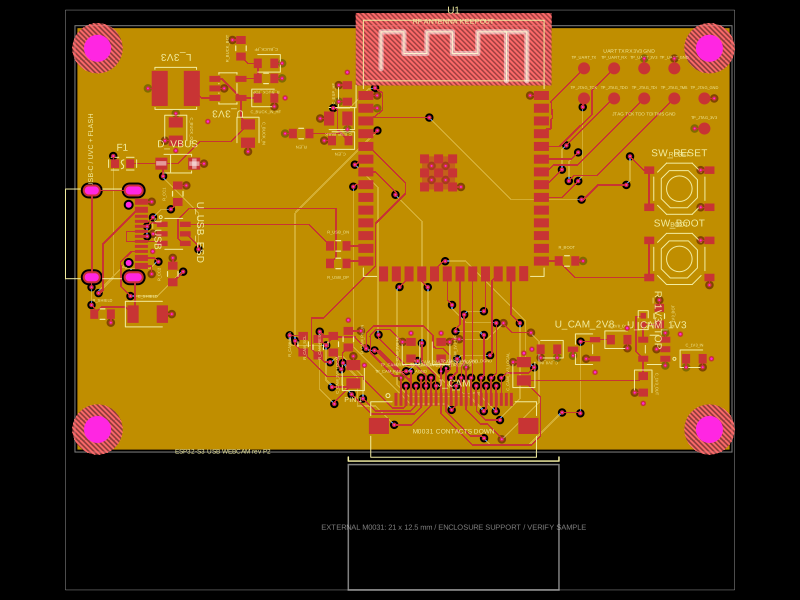 More from this author0hmX/esp32-s3-usb-webcam-ov2640This code defines and integrates a variety of surface-mount, through-hole, and connector hardware components (including microcontrollers, regulators, resistors, capacitors, and connectors) into a PCB design framework, enabling schematic symbol creation, footprint definition, and automated routing within an electronic circuit layout.
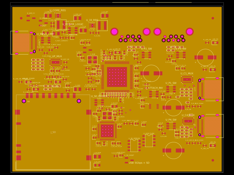 Similar packagegokul/usb3-sd-hubEngineering draft: four-layer, computer-powered USB 3 hub with one USB-C host socket, two USB-C and two USB-A accessory sockets, and a full-size SD slot. Board and three schematic previews are available. Routing and production checks are incomplete; not fabrication ready.
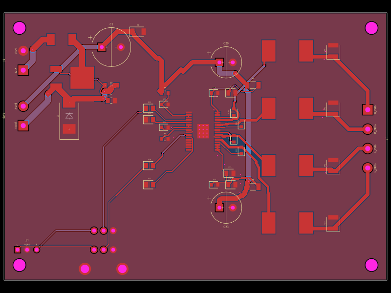 Discover something newhuntiep/radioA 12‑V car-powered stereo aux amplifier PCB using a TPA3118D2 class‑D BTL amp, protected power input, dual-gang volume control, LC speaker filters, and four-wire left/right speaker outputs.