0hmX/am3352-ddr-track-a-local-dfm-wip-20261007
Experimental RJ45-corrected board with isolated PG indication. 1005/1005 source joins pass; 15 expanded-guard physical errors, sourcing and qualification gates remain. Not fabrication-ready.
- Version
- 0.0.14
- License
- unset
- Stars
- 0
data/usb-c-ports.tsx
/**
 * Two USB-C ports:
 *
 * 1. J_POWER (existing receptacle, "Power input" sheet) becomes a USB PD sink. The
 *    TUSB320LAI current detector is replaced by an Infineon EZ-PD BCR CYPD3177-24LQXQ
 *    that negotiates a fixed 5 V / 3 A contract (SYS_5V and everything below it stay
 *    5 V). The existing TPS259531 eFuse still does inrush/current limiting; its EN is now
 *    driven by the BCR's VBUS_FET_EN ("power contract within range"), inverted by the
 *    existing SN74LVC1G98 (In2 = In1 = GND, so Y = !In0).
 *    Datasheet: Infineon 002-25383 Rev *B (EZ-PD BCR), Table 1 pinout, Tables 2-4 dividers,
 *    Figure 4 package (002-16934 *C, 4x4mm QFN-24, e 0.5, EP 2.75 nom).
 *      VBUS_MIN = VBUS_MAX = 5 V: pin tied to GND (ratio 0/6, Table 2)
 *      ISNK_COARSE = 3 A: 5.1k up from VDDD / 5.1k down (ratio 3/6, Table 3)
 *      ISNK_FINE = +0: tied to GND (Table 4)
 *      VDDD: 1 uF + 2 x 100 nF, VCCD: 1 uF, VBUS_IN: 1 uF (Table 1, Figure 3)
 *    HPI (I2C) is unused: SDA/SCL held at VDDD. FLIP has no pull-up (UFP VDO data bit = 1).
 *
 * 2. J_USB_PROG (new, "USB programming" sheet): USB 2.0 device port on AM3352 USB0
 *    (ROM USB/RNDIS boot for flashing, Linux gadget serial/ethernet afterwards).
 *    5.1k Rd on CC1/CC2, ESD204 on D+/D-, both connector D+/D- pairs joined.
 *    USB0 balls (ZCZ): DP N17, DM N18, VBUS P15 (VBUS sense only; this port never
 *    powers the board). USB0_ID P16 left open = B-device.
 */

// ---------- 1. PD sink on J_POWER ----------

/** Parts dropped from the Power input sheet (TUSB320 path). */
export const removedPowerParts = ["U_TYPEC", "R_TYPEC_VBUS", "R_TYPEC_OUT1", "R_TYPEC_OUT2"]

/** SN74LVC1G98 re-strapped as an inverter of VBUS_FET_EN (active-low contract OK). */
export const connectionOverrides: Record<string, Record<string, string>> = {
  U_TYPEC_NOR: { "1": "GND", "2": "GND", "3": "PD_CONTRACT_N", "4": "TYPEC_3A_OK", "5": "USBC_VBUS_RAW", "6": "GND" },
}

const powerSheet = "Power input"
const c0402 = (name: string, value: string, mpn: string, net: string, sheet: string) => ({
  name, kind: "capacitor", value, mpn, sheet, footprint: "0402",
  pinLabels: { "1": "1", "2": "2" }, noConnect: [], connections: { "1": "GND", "2": net },
})
const r0402 = (name: string, value: string, a: string, b: string, sheet: string) => ({
  name, kind: "resistor", value, sheet, footprint: "0402",
  pinLabels: { "1": "1", "2": "2" }, noConnect: [], connections: { "1": a, "2": b },
})

export const pdParts = [
  {
    name: "U_PD", kind: "chip", value: "CYPD3177-24LQXQ", mpn: "CYPD3177-24LQXQ", sheet: powerSheet,
    package: "QFN-24 4x4mm (002-16934)", footprintKey: "CYPD3177_QFN24",
    notes: "USB PD sink, fixed 5 V / 3 A request. VBUS_FET_EN low = contract within range.",
    pinLabels: {
      "1": "VBUS_MIN", "2": "VBUS_MAX", "3": "VBUS_FET_EN", "4": "SAFE_PWR_EN", "5": "ISNK_COARSE", "6": "ISNK_FINE",
      "7": "HPI_INT", "8": "GPIO_1", "9": "FAULT", "10": "FLIP", "11": "VDC_OUT", "12": "HPI_SDA",
      "13": "HPI_SCL", "14": "CC2", "15": "CC1", "16": "DM", "17": "DP", "18": "VBUS_IN",
      "19": "GND", "20": "DNU1", "21": "DNU2", "22": "VSS", "23": "VDDD", "24": "VCCD", "25": "EPAD",
    },
    noConnect: ["4", "7", "8", "9", "10", "16", "17", "20", "21"],
    connections: {
      "1": "GND", "2": "GND", "3": "PD_CONTRACT_N", "5": "PD_ISNK_COARSE", "6": "GND",
      "11": "SYS_5V", "12": "PD_VDDD", "13": "PD_VDDD", "14": "USBC_CC2", "15": "USBC_CC1",
      "18": "USBC_VBUS_RAW", "19": "GND", "22": "GND", "23": "PD_VDDD", "24": "PD_VCCD", "25": "GND",
    },
  },
  c0402("C_PD_VBUS", "1uF", "GRM155R61C105KA12D", "USBC_VBUS_RAW", powerSheet),
  c0402("C_PD_VDDD", "1uF", "GRM155R61C105KA12D", "PD_VDDD", powerSheet),
  c0402("C_PD_VDDD_HF1", "100nF", "GRM155R71C104KA88D", "PD_VDDD", powerSheet),
  c0402("C_PD_VDDD_HF2", "100nF", "GRM155R71C104KA88D", "PD_VDDD", powerSheet),
  c0402("C_PD_VCCD", "1uF", "GRM155R61C105KA12D", "PD_VCCD", powerSheet),
  r0402("R_PD_ISNK_UP", "5.1k", "PD_VDDD", "PD_ISNK_COARSE", powerSheet),
  r0402("R_PD_ISNK_DN", "5.1k", "GND", "PD_ISNK_COARSE", powerSheet),
]

type Place = { pcbX: number; pcbY: number; pcbRotation: number; layer: "top"; isAllowedToBeOffBoard?: boolean }

/** Free top-edge pocket west of the eFuse (x 0..9.5, y 20.6..26.5 is empty on all routing layers). */
export const pdPlacement: Record<string, Place> = {
  U_PD: { pcbX: 6, pcbY: 23, pcbRotation: 0, layer: "top" },
  C_PD_VBUS: { pcbX: 9.3, pcbY: 25.4, pcbRotation: 0, layer: "top" },
  C_PD_VCCD: { pcbX: 3.4, pcbY: 25.85, pcbRotation: 0, layer: "top" },
  C_PD_VDDD: { pcbX: 1.4, pcbY: 25.85, pcbRotation: 0, layer: "top" },
  C_PD_VDDD_HF1: { pcbX: 1.4, pcbY: 24.8, pcbRotation: 0, layer: "top" },
  C_PD_VDDD_HF2: { pcbX: 1.4, pcbY: 23.8, pcbRotation: 0, layer: "top" },
  R_PD_ISNK_UP: { pcbX: 1.4, pcbY: 22.8, pcbRotation: 0, layer: "top" },
  R_PD_ISNK_DN: { pcbX: 1.4, pcbY: 21.8, pcbRotation: 0, layer: "top" },
}

// KiCad Package_DFN_QFN.pretty/QFN-24-1EP_4x4mm_P0.5mm_EP2.75x2.75mm, Y flipped to +Y up.
// Matches the Cypress 002-16934 drawing (b 0.25, L 0.40, e 0.50, D2/E2 2.75 nom).
const qfnPads = [
  ...[0, 1, 2, 3, 4, 5].map(k => ({ pin: String(1 + k), x: -1.975, y: 1.25 - 0.5 * k, width: 0.8, height: 0.25 })),
  ...[0, 1, 2, 3, 4, 5].map(k => ({ pin: String(7 + k), x: -1.25 + 0.5 * k, y: -1.975, width: 0.25, height: 0.8 })),
  ...[0, 1, 2, 3, 4, 5].map(k => ({ pin: String(13 + k), x: 1.975, y: -1.25 + 0.5 * k, width: 0.8, height: 0.25 })),
  ...[0, 1, 2, 3, 4, 5].map(k => ({ pin: String(19 + k), x: 1.25 - 0.5 * k, y: 1.975, width: 0.25, height: 0.8 })),
  { pin: "25", x: 0, y: 0, width: 2.75, height: 2.75 },
].map(p => ({ ...p, type: "smd", shape: "roundrect", rotation: 0, drill: null }))

// ---------- 2. USB0 programming port ----------

export const progSheet = "USB programming"

export const progParts = [
  {
    name: "J_USB_PROG", kind: "chip", mpn: "USB4105-GF-A", sheet: progSheet, footprintKey: "USBC",
    source: "https://gct.co/files/drawings/usb4105.pdf",
    pinLabels: { A1: "GND", A4: "VBUS", A5: "CC1", A6: "DP1", A7: "DM1", A8: "SBU1", A9: "VBUS", A12: "GND",
      B1: "GND", B4: "VBUS", B5: "CC2", B6: "DP2", B7: "DM2", B8: "SBU2", B9: "VBUS", B12: "GND", SH: "SHIELD" },
    noConnect: ["A8", "B8"],
    connections: {
      A1: "GND", A12: "GND", B1: "GND", B12: "GND", SH: "GND",
      A4: "USB0_VBUS", A9: "USB0_VBUS", B4: "USB0_VBUS", B9: "USB0_VBUS",
      A5: "USB_PROG_CC1", B5: "USB_PROG_CC2",
      A6: "USB0_DP", B6: "USB0_DP", A7: "USB0_DM", B7: "USB0_DM",
    },
  },
  r0402("R_PROG_CC1", "5.1k", "USB_PROG_CC1", "GND", progSheet),
  r0402("R_PROG_CC2", "5.1k", "USB_PROG_CC2", "GND", progSheet),
  {
    name: "U_PROG_ESD", kind: "chip", mpn: "ESD204DQAR", sheet: progSheet, footprintKey: "ESD204_DQA",
    pinLabels: { "1": "IO1", "2": "IO2", "3": "GND", "4": "IO3", "5": "IO4", "6": "NC", "7": "NC", "8": "GND", "9": "NC", "10": "NC" },
    noConnect: ["4", "5", "6", "7", "9", "10"],
    connections: { "1": "USB0_DP", "2": "USB0_DM", "3": "GND", "8": "GND" },
  },
]

/** Top-left corner: free on every copper layer; same edge and depth as J_POWER. */
export const progPlacement: Record<string, Place> = {
  J_USB_PROG: { pcbX: -17, pcbY: 22.825, pcbRotation: 180, layer: "top", isAllowedToBeOffBoard: true },
  U_PROG_ESD: { pcbX: -17, pcbY: 16.6, pcbRotation: 90, layer: "top" },
  R_PROG_CC1: { pcbX: -14.2, pcbY: 17, pcbRotation: 90, layer: "top" },
  R_PROG_CC2: { pcbX: -20.4, pcbY: 17, pcbRotation: 90, layer: "top" },
}

export const usbCPortParts = [...pdParts, ...progParts]
export const usbCPortPlacement = { ...pdPlacement, ...progPlacement }
export const usbCPortFootprints = {
  CYPD3177_QFN24: { source: "Package_DFN_QFN.pretty/QFN-24-1EP_4x4mm_P0.5mm_EP2.75x2.75mm.kicad_mod", pads: qfnPads },
}
/** KiCad F.CrtYd: [minX, minY, maxX, maxY] */
export const usbCPortCourtyards = { CYPD3177_QFN24: { bounds: [-2.63, -2.63, 2.63, 2.63] } }
Related Packages
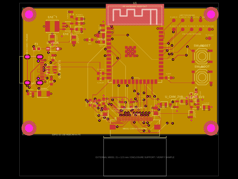 More from this author0hmX/esp32-s3-usb-webcam-ov2640This code defines and integrates a variety of surface-mount, through-hole, and connector hardware components (including microcontrollers, regulators, resistors, capacitors, and connectors) into a PCB design framework, enabling schematic symbol creation, footprint definition, and automated routing within an electronic circuit layout.
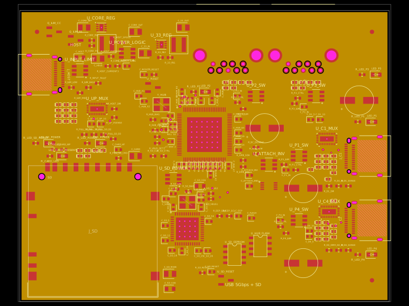 Similar packagegokul/usb3-sd-hubEngineering draft: four-layer, computer-powered USB 3 hub with one USB-C host socket, two USB-C and two USB-A accessory sockets, and a full-size SD slot. Board and three schematic previews are available. Routing and production checks are incomplete; not fabrication ready.
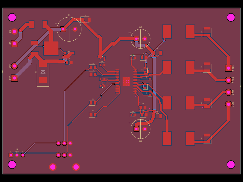 Discover something newhuntiep/radioA 12‑V car-powered stereo aux amplifier PCB using a TPA3118D2 class‑D BTL amp, protected power input, dual-gang volume control, LC speaker filters, and four-wire left/right speaker outputs.