tscircuit/boosters
This code defines PCB schematics, footprints, and 3D CAD models for various integrated circuits, connectors, sensors, and electronic components used in TI booster packs and modules.
- Version
- 0.1.19
- License
- unset
- Stars
- 0
tida-00647/index.circuit.tsx
PCB

Schematic

import { ADS1220IRVAR } from "./imports/ADS1220IRVAR"
import { DB125_3_5_4P_GN_S } from "./imports/DB125_3_5_4P_GN_S"
import { SSQ_110_03_G_D } from "./imports/SSQ_110_03_G_D"
import { TSW_102_07_G_S } from "./imports/TSW_102_07_G_S"
import { ZHCS350TA } from "./imports/ZHCS350TA"

export default () => (
  <board
    title="TI TIDA-00647 ADS1220 RTD BoosterPack"
    width="58.42mm"
    height="28.702mm"
    layers={2}
    thickness="1.6mm"
    solderMaskColor="green"
    silkscreenColor="white"
    minViaHoleDiameter="0.4064mm"
    minViaPadDiameter="0.8636mm"
  >
    <schematicsheet
      name="ADC and LaunchPad interface"
      displayName="ADC and LaunchPad interface"
      sheetIndex={1}
    />
    <schematicsheet
      name="RTD analog front end"
      displayName="RTD analog front end"
      sheetIndex={2}
    />

    {/* TI TIDA-00647 component identities and positions from ADS1220_RTD_BP.PcbDoc. */}
    <ADS1220IRVAR
      name="U1"
      pcbX={0.82}
      pcbY={-0.9287}
      pcbRotation={270}
      schX={-0.6}
      schY={0}
      schWidth="3mm"
      schHeight="1.4mm"
      schSheetName="ADC and LaunchPad interface"
      schPinArrangement={{
        leftSide: {
          pins: ["CLK", "CSN", "SCLK", "DIN", "DOUT_DRDY", "DRDYN"],
          direction: "top-to-bottom",
        },
        rightSide: {
          pins: [
            "AIN0_REFP1",
            "AIN1",
            "AIN2",
            "AIN3_REFN1",
            "REFP0",
            "REFN0",
            "AVDD",
            "DVDD",
            "DGND",
            "AVSS",
            "EP",
          ],
          direction: "top-to-bottom",
        },
      }}
    />

    {/* The native Altium J1 footprint is the two physical BoosterPack sockets. */}
    <SSQ_110_03_G_D
      name="J1A"
      manufacturerPartNumber="SSW-110-23-F-D"
      pcbX={-21.52260364}
      pcbY={-0.11360404}
      pcbRotation={90}
      schX={-8}
      schY={0}
      schWidth="2.5mm"
      schHeight="2.2mm"
      schSheetName="ADC and LaunchPad interface"
      schPinArrangement={{
        leftSide: {
          pins: [
            "pin1",
            "pin3",
            "pin5",
            "pin7",
            "pin9",
            "pin11",
            "pin13",
            "pin15",
            "pin17",
            "pin19",
          ],
          direction: "top-to-bottom",
        },
        rightSide: {
          pins: [
            "pin2",
            "pin4",
            "pin6",
            "pin8",
            "pin10",
            "pin12",
            "pin14",
            "pin16",
            "pin18",
            "pin20",
          ],
          direction: "top-to-bottom",
        },
      }}
    />
    <SSQ_110_03_G_D
      name="J1B"
      manufacturerPartNumber="SSW-110-23-F-D"
      pcbX={21.65739636}
      pcbY={-0.11360404}
      pcbRotation={90}
      schX={8}
      schY={0}
      schWidth="2.5mm"
      schHeight="2.2mm"
      schSheetName="ADC and LaunchPad interface"
      schPinArrangement={{
        leftSide: {
          pins: [
            "pin1",
            "pin3",
            "pin5",
            "pin7",
            "pin9",
            "pin11",
            "pin13",
            "pin15",
            "pin17",
            "pin19",
          ],
          direction: "top-to-bottom",
        },
        rightSide: {
          pins: [
            "pin2",
            "pin4",
            "pin6",
            "pin8",
            "pin10",
            "pin12",
            "pin14",
            "pin16",
            "pin18",
            "pin20",
          ],
          direction: "top-to-bottom",
        },
      }}
    />

    <DB125_3_5_4P_GN_S
      name="J2"
      manufacturerPartNumber="ED555/4DS"
      pcbX={-2.02959589}
      pcbY={10.06815106}
      pcbRotation={180}
      schX={-7}
      schY={0}
      schWidth="2.2mm"
      schHeight="1mm"
      schSheetName="RTD analog front end"
      schPinArrangement={{
        rightSide: {
          pins: ["pin1", "pin2", "pin3", "pin4"],
          direction: "top-to-bottom",
        },
      }}
    />
    <TSW_102_07_G_S
      name="J3"
      pcbX={3.42}
      pcbY={4.45}
      pcbRotation={0}
      schX={-4.5}
      schY={2.5}
      schWidth="1.8mm"
      schHeight="0.4mm"
      schSheetName="RTD analog front end"
    />
    <TSW_102_07_G_S
      name="J4"
      pcbX={-5.42}
      pcbY={4.51}
      pcbRotation={180}
      schX={-4.5}
      schY={-2.5}
      schWidth="1.8mm"
      schHeight="0.4mm"
      schSheetName="RTD analog front end"
    />

    <resistor
      name="R1"
      resistance="4.22k"
      footprint="0805"
      manufacturerPartNumber="RG2012P-4221-B-T5"
      pcbX={-5.9}
      pcbY={-1.94469996}
      pcbRotation={0}
      schX={-1.5}
      schY={3.6}
      schSheetName="RTD analog front end"
    />
    <resistor
      name="R2"
      resistance="3.24k"
      footprint="1206"
      manufacturerPartNumber="PFC-W1206R-12-3241-B"
      pcbX={-6.02860404}
      pcbY={-4.35769996}
      pcbRotation={180}
      schX={-3.5}
      schY={0}
      schSheetName="RTD analog front end"
    />
    <resistor
      name="R3"
      resistance="4.22k"
      footprint="0805"
      manufacturerPartNumber="RG2012P-4221-B-T5"
      pcbX={-5.52060404}
      pcbY={0.21430004}
      pcbRotation={0}
      schX={-1.5}
      schY={2.1}
      schSheetName="RTD analog front end"
    />
    <resistor
      name="R4"
      resistance="10k"
      footprint="0402"
      manufacturerPartNumber="CRCW040210K0FKEDHP"
      pcbX={3.65}
      pcbY={1.5}
      pcbRotation={270}
      schX={-3.2}
      schY={2.7}
      schSheetName="ADC and LaunchPad interface"
    />
    <resistor
      name="R5"
      resistance="0"
      footprint="0402"
      manufacturerPartNumber="CRCW04020000Z0ED"
      pcbX={9.839787}
      pcbY={2.600231}
      pcbRotation={0}
      schX={4.1}
      schY={2.8}
      schSheetName="ADC and LaunchPad interface"
    />
    <resistor
      name="R6"
      resistance="0"
      footprint="0402"
      manufacturerPartNumber="CRCW04020000Z0ED"
      pcbX={9.839797}
      pcbY={1.330241}
      pcbRotation={0}
      schX={4.1}
      schY={1.4}
      schSheetName="ADC and LaunchPad interface"
    />
    <resistor
      name="R7"
      resistance="0"
      footprint="0402"
      manufacturerPartNumber="CRCW04020000Z0ED"
      pcbX={9.839792}
      pcbY={-1.336769}
      pcbRotation={180}
      schX={4.7}
      schY={0}
      schSheetName="ADC and LaunchPad interface"
    />
    <resistor
      name="R8"
      resistance="0"
      footprint="0402"
      manufacturerPartNumber="CRCW04020000Z0ED"
      pcbX={9.839792}
      pcbY={0.060231}
      pcbRotation={0}
      schX={4.1}
      schY={-1.4}
      schSheetName="ADC and LaunchPad interface"
    />
    <resistor
      name="R9"
      resistance="4.22k"
      footprint="0805"
      manufacturerPartNumber="RG2012P-4221-B-T5"
      pcbX={0.70239596}
      pcbY={-8.29469996}
      pcbRotation={90}
      schX={0}
      schY={-0.8}
      schSheetName="RTD analog front end"
    />
    <resistor
      name="R10"
      resistance="0"
      footprint="0402"
      manufacturerPartNumber="CRCW04020000Z0ED"
      pcbX={9.839792}
      pcbY={-2.606769}
      pcbRotation={180}
      schX={4.1}
      schY={-2.8}
      schSheetName="ADC and LaunchPad interface"
    />
    <resistor
      name="R11"
      resistance="4.22k"
      footprint="0805"
      manufacturerPartNumber="RG2012P-4221-B-T5"
      pcbX={-1.58360404}
      pcbY={-8.29469996}
      pcbRotation={90}
      schX={0}
      schY={-3.3}
      schSheetName="RTD analog front end"
    />

    <capacitor
      name="C1"
      capacitance="1800pF"
      footprint="0603"
      manufacturerPartNumber="GRM188R72A182KA01D"
      pcbX={-2.6}
      pcbY={-4.35769996}
      pcbRotation={270}
      schX={1.3}
      schY={3.6}
      schOrientation="vertical"
      schSheetName="RTD analog front end"
    />
    <capacitor
      name="C2"
      capacitance="0.018uF"
      footprint="0603"
      manufacturerPartNumber="C0603C183K1RACTU"
      pcbX={-2.6}
      pcbY={-1.05569996}
      pcbRotation={90}
      schX={1.3}
      schY={2.1}
      schOrientation="vertical"
      schSheetName="RTD analog front end"
    />
    <capacitor
      name="C3"
      capacitance="1800pF"
      footprint="0603"
      manufacturerPartNumber="GRM188R72A182KA01D"
      pcbX={-4.4}
      pcbY={2.24630004}
      pcbRotation={180}
      schX={1.3}
      schY={0.6}
      schOrientation="vertical"
      schSheetName="RTD analog front end"
    />
    <capacitor
      name="C4"
      capacitance="2700pF"
      footprint="0603"
      manufacturerPartNumber="GRM188R72A272KA01D"
      pcbX={3.49639596}
      pcbY={-7.27869996}
      pcbRotation={0}
      schX={2.5}
      schY={-0.8}
      schOrientation="vertical"
      schSheetName="RTD analog front end"
    />
    <capacitor
      name="C5"
      capacitance="0.027uF"
      footprint="0603"
      manufacturerPartNumber="C0603C273K1RACTU"
      pcbX={-0.31360404}
      pcbY={-5.50069996}
      pcbRotation={180}
      schX={2.5}
      schY={-2.05}
      schOrientation="vertical"
      schSheetName="RTD analog front end"
    />
    <capacitor
      name="C6"
      capacitance="2700pF"
      footprint="0603"
      manufacturerPartNumber="GRM188R72A272KA01D"
      pcbX={-3.48860404}
      pcbY={-8.29469996}
      pcbRotation={90}
      schX={2.5}
      schY={-3.3}
      schOrientation="vertical"
      schSheetName="RTD analog front end"
    />
    <capacitor
      name="C7"
      capacitance="0.1uF"
      footprint="0603"
      manufacturerPartNumber="C0603X104K4RACTU"
      pcbX={2.48039596}
      pcbY={-4.8}
      pcbRotation={270}
      schX={-1.4}
      schY={-4.4}
      schOrientation="vertical"
      schSheetName="ADC and LaunchPad interface"
    />
    <capacitor
      name="C8"
      capacitance="0.1uF"
      footprint="0603"
      manufacturerPartNumber="C0603X104K4RACTU"
      pcbX={-14.605}
      pcbY={11.811}
      pcbRotation={270}
      schX={1.4}
      schY={-4.4}
      schOrientation="vertical"
      schSheetName="ADC and LaunchPad interface"
    />

    <ZHCS350TA
      name="D1"
      pcbX={-1.81060404}
      pcbY={2.75430004}
      pcbRotation={270}
      schX={5}
      schY={-1.3}
      schSheetName="RTD analog front end"
    />
    <ZHCS350TA
      name="D2"
      pcbX={-0.21360404}
      pcbY={2.75430004}
      pcbRotation={270}
      schX={5}
      schY={-3.8}
      schSheetName="RTD analog front end"
    />

    {/* LaunchPad digital interface. J1A/J1B pad numbers preserve TI J1 positions. */}
    <trace from=".J1A > .pin8" to="net.SPI_CLK" width="0.254mm" schDisplayLabel="SPI_CLK" />
    <trace from=".R6 > .pin2" to="net.SPI_CLK" width="0.254mm" schDisplayLabel="SPI_CLK" />
    <trace from=".R6 > .pin1" to="net.ADS_SCLK" width="0.254mm" schDisplayLabel="ADS_SCLK" />
    <trace from=".U1 > .SCLK" to="net.ADS_SCLK" width="0.254mm" schDisplayLabel="ADS_SCLK" />

    <trace from=".J1B > .pin9" to="net.SPI_MOSI" width="0.254mm" schDisplayLabel="SPI_MOSI" />
    <trace from=".R8 > .pin2" to="net.SPI_MOSI" width="0.254mm" schDisplayLabel="SPI_MOSI" />
    <trace from=".R8 > .pin1" to="net.ADS_DIN" width="0.254mm" schDisplayLabel="ADS_DIN" />
    <trace from=".U1 > .DIN" to="net.ADS_DIN" width="0.254mm" schDisplayLabel="ADS_DIN" />

    <trace from=".J1B > .pin7" to="net.SPI_MISO" width="0.254mm" schDisplayLabel="SPI_MISO" />
    <trace from=".R7 > .pin1" to="net.SPI_MISO" width="0.254mm" schDisplayLabel="SPI_MISO" />
    <trace from=".R7 > .pin2" to="net.ADS_DOUT" width="0.254mm" schDisplayLabel="ADS_DOUT" />
    <trace from=".U1 > .DOUT_DRDY" to="net.ADS_DOUT" width="0.254mm" schDisplayLabel="ADS_DOUT" />

    <trace from=".J1B > .pin1" to="net.ADS_CS" width="0.254mm" schDisplayLabel="ADS_CS" />
    <trace from=".R5 > .pin2" to="net.ADS_CS" width="0.254mm" schDisplayLabel="ADS_CS" />
    <trace from=".R5 > .pin1" to="net.ADS_CSN" width="0.254mm" schDisplayLabel="ADS_CSN" />
    <trace from=".U1 > .CSN" to="net.ADS_CSN" width="0.254mm" schDisplayLabel="ADS_CSN" />

    <trace from=".J1B > .pin15" to="net.ADS_DRDY" width="0.254mm" schDisplayLabel="ADS_DRDY" />
    <trace from=".R10 > .pin1" to="net.ADS_DRDY" width="0.254mm" schDisplayLabel="ADS_DRDY" />
    <trace from=".R10 > .pin2" to="net.ADS_DRDYN" width="0.254mm" schDisplayLabel="ADS_DRDYN" />
    <trace from=".U1 > .DRDYN" to="net.ADS_DRDYN" width="0.254mm" schDisplayLabel="ADS_DRDYN" />

    <trace from=".R4 > .pin2" to="net.ADS_CLK" width="0.254mm" schDisplayLabel="ADS_CLK" />
    <trace from=".U1 > .CLK" to="net.ADS_CLK" width="0.254mm" schDisplayLabel="ADS_CLK" />
    <trace from=".R4 > .pin1" to="net.GND" width="0.254mm" schDisplayLabel="GND" />

    {/* Supply routing. TI uses 20 mil for the main 3.3 V distribution. */}
    <trace from=".J1A > .pin20" to="net.V3P3" width="0.508mm" schDisplayLabel="+3V3" />
    <trace from=".U1 > .AVDD" to="net.V3P3" width="0.508mm" schDisplayLabel="+3V3" />
    <trace from=".U1 > .DVDD" to="net.V3P3" width="0.508mm" schDisplayLabel="+3V3" />
    <trace from=".C7 > .pin1" to="net.V3P3" width="0.508mm" schDisplayLabel="+3V3" />
    <trace from=".C8 > .pin1" to="net.V3P3" width="0.508mm" schDisplayLabel="+3V3" />
    <trace from=".J1A > .pin19" to="net.V5" width="0.254mm" schDisplayLabel="+5V" />

    <trace from=".J1A > .pin17" to="net.GND" width="0.254mm" schDisplayLabel="GND" />
    <trace from=".J1B > .pin19" to="net.GND" width="0.254mm" schDisplayLabel="GND" />
    <trace from=".U1 > .DGND" to="net.GND" width="0.254mm" schDisplayLabel="GND" />
    <trace from=".U1 > .AVSS" to="net.GND" width="0.254mm" schDisplayLabel="GND" />
    <trace from=".U1 > .EP" to="net.GND" width="0.254mm" schDisplayLabel="GND" />
    <trace from=".C7 > .pin2" to="net.GND" width="0.254mm" schDisplayLabel="GND" />
    <trace from=".C8 > .pin2" to="net.GND" width="0.254mm" schDisplayLabel="GND" />
    <trace from=".C1 > .pin2" to="net.GND" width="0.254mm" schDisplayLabel="GND" />
    <trace from=".C3 > .pin1" to="net.GND" width="0.254mm" schDisplayLabel="GND" />
    <trace from=".R3 > .pin1" to="net.GND" width="0.254mm" schDisplayLabel="GND" />
    <trace from=".R2 > .pin1" to="net.GND" width="0.254mm" schDisplayLabel="GND" />
    <trace from=".C4 > .pin2" to="net.GND" width="0.254mm" schDisplayLabel="GND" />
    <trace from=".C6 > .pin1" to="net.GND" width="0.254mm" schDisplayLabel="GND" />

    {/* ADS1220 reference network. */}
    <trace from=".U1 > .REFP0" to="net.ADS_REFP0" width="0.254mm" schDisplayLabel="ADS_REFP0" />
    <trace from=".C2 > .pin1" to="net.ADS_REFP0" width="0.254mm" schDisplayLabel="ADS_REFP0" />
    <trace from=".C1 > .pin1" to="net.ADS_REFP0" width="0.254mm" schDisplayLabel="ADS_REFP0" />
    <trace from=".R1 > .pin2" to="net.ADS_REFP0" width="0.254mm" schDisplayLabel="ADS_REFP0" />

    <trace from=".U1 > .REFN0" to="net.ADS_REFN0" width="0.254mm" schDisplayLabel="ADS_REFN0" />
    <trace from=".C2 > .pin2" to="net.ADS_REFN0" width="0.254mm" schDisplayLabel="ADS_REFN0" />
    <trace from=".C3 > .pin2" to="net.ADS_REFN0" width="0.254mm" schDisplayLabel="ADS_REFN0" />
    <trace from=".R3 > .pin2" to="net.ADS_REFN0" width="0.254mm" schDisplayLabel="ADS_REFN0" />

    {/* Four-wire RTD terminal and 2-/3-wire configuration headers. */}
    <trace from=".J3 > .pin2" to="net.RTD_REF" width="0.254mm" schDisplayLabel="RTD_REF" />
    <trace from=".J2 > .pin1" to="net.RTD_REF" width="0.254mm" schDisplayLabel="RTD_REF" />
    <trace from=".R1 > .pin1" to="net.RTD_REF" width="0.254mm" schDisplayLabel="RTD_REF" />
    <trace from=".R2 > .pin2" to="net.RTD_REF" width="0.254mm" schDisplayLabel="RTD_REF" />

    <trace from=".J4 > .pin1" to="net.RTD_SENSE3" width="0.254mm" schDisplayLabel="RTD_SENSE3" />
    <trace from=".J2 > .pin3" to="net.RTD_SENSE3" width="0.254mm" schDisplayLabel="RTD_SENSE3" />
    <trace from=".R9 > .pin1" to="net.RTD_SENSE3" width="0.254mm" schDisplayLabel="RTD_SENSE3" />

    <trace from=".J3 > .pin1" to="net.RTD_SENSE2" width="0.254mm" schDisplayLabel="RTD_SENSE2" />
    <trace from=".J2 > .pin2" to="net.RTD_SENSE2" width="0.254mm" schDisplayLabel="RTD_SENSE2" />
    <trace from=".D2 > .cathode" to="net.RTD_SENSE2" width="0.254mm" schDisplayLabel="RTD_SENSE2" />
    <trace from=".R11 > .pin1" to="net.RTD_SENSE2" width="0.254mm" schDisplayLabel="RTD_SENSE2" />

    <trace from=".J4 > .pin2" to="net.RTD_SENSE4" width="0.254mm" schDisplayLabel="RTD_SENSE4" />
    <trace from=".J2 > .pin4" to="net.RTD_SENSE4" width="0.254mm" schDisplayLabel="RTD_SENSE4" />
    <trace from=".D1 > .cathode" to="net.RTD_SENSE4" width="0.254mm" schDisplayLabel="RTD_SENSE4" />

    {/* Differential analog input filtering and protection. */}
    <trace from=".U1 > .AIN0_REFP1" to="net.ADS_AIN0" width="0.254mm" schDisplayLabel="ADS_AIN0" />
    <trace from=".C5 > .pin1" to="net.ADS_AIN0" width="0.254mm" schDisplayLabel="ADS_AIN0" />
    <trace from=".C4 > .pin1" to="net.ADS_AIN0" width="0.254mm" schDisplayLabel="ADS_AIN0" />
    <trace from=".R9 > .pin2" to="net.ADS_AIN0" width="0.254mm" schDisplayLabel="ADS_AIN0" />

    <trace from=".U1 > .AIN1" to="net.ADS_AIN1" width="0.254mm" schDisplayLabel="ADS_AIN1" />
    <trace from=".C5 > .pin2" to="net.ADS_AIN1" width="0.254mm" schDisplayLabel="ADS_AIN1" />
    <trace from=".C6 > .pin2" to="net.ADS_AIN1" width="0.254mm" schDisplayLabel="ADS_AIN1" />
    <trace from=".R11 > .pin2" to="net.ADS_AIN1" width="0.254mm" schDisplayLabel="ADS_AIN1" />

    <trace from=".U1 > .AIN2" to="net.ADS_AIN2" width="0.254mm" schDisplayLabel="ADS_AIN2" />
    <trace from=".D1 > .anode" to="net.ADS_AIN2" width="0.254mm" schDisplayLabel="ADS_AIN2" />

    <trace from=".U1 > .AIN3_REFN1" to="net.ADS_AIN3" width="0.254mm" schDisplayLabel="ADS_AIN3" />
    <trace from=".D2 > .anode" to="net.ADS_AIN3" width="0.254mm" schDisplayLabel="ADS_AIN3" />

    {/* The native design has one solid bottom-layer GND polygon. */}
    <copperpour
      name="GND_BOTTOM_POUR"
      connectsTo="net.GND"
      layer="bottom"
      clearance="0.254mm"
      padMargin="0.254mm"
      traceMargin="0.254mm"
      cutoutMargin="0.254mm"
      boardEdgeMargin="0.635mm"
      coveredWithSolderMask
      outline={[
        { x: -29.21, y: -14.351 },
        { x: 29.21, y: -14.351 },
        { x: 29.21, y: 14.351 },
        { x: -29.21, y: 14.351 },
        { x: -29.21, y: -14.351 },
      ]}
    />

  </board>
)
Related Packages
 More from this authortscircuit/autorouting-dataset-01This code manages the hardware and electronic components for circuit design and PCB layout, defining components like resistors, capacitors, transistors, connectors, and footprints, and providing tools for component placement, PCB topology, and electrical connections.
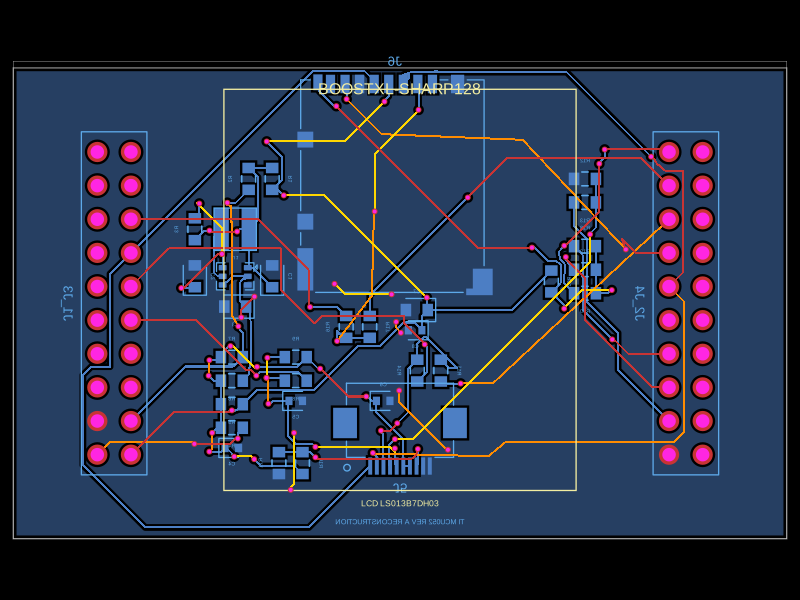 Similar packageabse/boostxl-sharp128This code defines a printed circuit board (PCB) with various surface-mount resistors, capacitors, inductors, and integrated circuits, including power management components and interface connectors, for a TI-based LCD and microSD module using 0603 and other package types.