tscircuit/boosters
This code defines PCB schematics, footprints, and 3D CAD models for various integrated circuits, connectors, sensors, and electronic components used in TI booster packs and modules.
- Version
- 0.1.19
- License
- unset
- Stars
- 0
boostxl-tmp107/index.circuit.tsx
PCB

Schematic

import { PZ254V_12_6P } from "./imports/PZ254V_12_6P"
import { SN74LVC1G07DBVR } from "./imports/SN74LVC1G07DBVR"
import { SSQ_110_03_T_D } from "./imports/SSQ_110_03_T_D"
import { TMP107BIDR } from "./imports/TMP107BIDR"

const N = {
  V5: "net.V5",
  V33: "net.V33",
  GND: "net.GND",
  RXD: "net.UCA0RXD",
  TXD: "net.UCA0TXD",
  TX_OD: "net.TX_OD",
  TX_R: "net.TX_R",
  BUS: "net.TMP_BUS",
  ALERT1: "net.ALERT1",
  ALERT2: "net.ALERT2",
  IO12: "net.IO1_2",
  IO13: "net.IO1_3",
  IO14: "net.IO1_4",
} as const

const HEADER_SCH_PIN_STYLE = {
  pin1: { marginTop: "0.05mm", marginBottom: "0.05mm" },
  pin2: { marginTop: "0.05mm", marginBottom: "0.05mm" },
  pin3: { marginTop: "0.05mm", marginBottom: "0.05mm" },
  pin4: { marginTop: "0.05mm", marginBottom: "0.05mm" },
  pin5: { marginTop: "0.05mm", marginBottom: "0.05mm" },
  pin6: { marginTop: "0.05mm", marginBottom: "0.05mm" },
  pin7: { marginTop: "0.05mm", marginBottom: "0.05mm" },
  pin8: { marginTop: "0.05mm", marginBottom: "0.05mm" },
  pin9: { marginTop: "0.05mm", marginBottom: "0.05mm" },
  pin10: { marginTop: "0.05mm", marginBottom: "0.05mm" },
  pin11: { marginTop: "0.05mm", marginBottom: "0.05mm" },
  pin12: { marginTop: "0.05mm", marginBottom: "0.05mm" },
  pin13: { marginTop: "0.05mm", marginBottom: "0.05mm" },
  pin14: { marginTop: "0.05mm", marginBottom: "0.05mm" },
  pin15: { marginTop: "0.05mm", marginBottom: "0.05mm" },
  pin16: { marginTop: "0.05mm", marginBottom: "0.05mm" },
  pin17: { marginTop: "0.05mm", marginBottom: "0.05mm" },
  pin18: { marginTop: "0.05mm", marginBottom: "0.05mm" },
  pin19: { marginTop: "0.05mm", marginBottom: "0.05mm" },
  pin20: { marginTop: "0.05mm", marginBottom: "0.05mm" },
}

const TMP107_SCH_PIN_STYLE = {
  pin1: { marginTop: "0.075mm", marginBottom: "0.075mm" },
  pin2: { marginTop: "0.075mm", marginBottom: "0.075mm" },
  pin3: { marginTop: "0.075mm", marginBottom: "0.075mm" },
  pin4: { marginTop: "0.075mm", marginBottom: "0.075mm" },
  pin5: { marginTop: "0.075mm", marginBottom: "0.075mm" },
  pin6: { marginTop: "0.075mm", marginBottom: "0.075mm" },
  pin7: { marginTop: "0.075mm", marginBottom: "0.075mm" },
  pin8: { marginTop: "0.075mm", marginBottom: "0.075mm" },
}

const SHUNT_HEADER_SCH_PIN_STYLE = {
  pin1: { marginTop: "0.15mm", marginBottom: "0.15mm" },
  pin2: { marginTop: "0.15mm", marginBottom: "0.15mm" },
  pin3: { marginTop: "0.15mm", marginBottom: "0.15mm" },
  pin4: { marginTop: "0.15mm", marginBottom: "0.15mm" },
  pin5: { marginTop: "0.15mm", marginBottom: "0.15mm" },
  pin6: { marginTop: "0.15mm", marginBottom: "0.15mm" },
}

export default function Circuit() {
  return (
    <board
      name="BOOSTXL_TMP107"
      width="53.34mm"
      height="40.64mm"
      outline={[
        { x: -26.67, y: -20.32 },
        { x: 26.67, y: -20.32 },
        { x: 26.67, y: 20.32 },
        { x: -26.67, y: 20.32 },
      ]}
      solderMaskColor="red"
      silkscreenColor="white"
      defaultTraceWidth="0.2mm"
      minViaHoleDiameter="0.3mm"
      minViaPadDiameter="0.45mm"
      autorouter={{
        preset: "auto_local",
        local: true,
        traceClearance: "0.15mm",
      }}
      autorouterEffortLevel="2x"
    >
      <schematicsheet
        name="BOOSTXL-TMP107 Complete Schematic"
        displayName="BOOSTXL-TMP107 Complete Schematic"
        sheetIndex={1}
      />

      <group
        name="COMPLETE_SCHEMATIC"
        schSheetName="BOOSTXL-TMP107 Complete Schematic"
        schX={0}
        schY={0}
        pcbX={0}
        pcbY={0}
        schMaxTraceDistance="1.2mm"
        schTraceAutoLabelEnabled
      >
        <schematicsection
          name="TI_MHR035_FUNCTIONAL_CIRCUIT"
          displayName="TI MHR035 Rev A functional circuit"
          sectionTitleFontSize="0.18mm"
        />
        <SSQ_110_03_T_D
          name="J1"
          layer="bottom"
          schSectionName="TI_MHR035_FUNCTIONAL_CIRCUIT"
          schX={-9.5}
          schY={7.2}
          schWidth="5.2mm"
          schHeight="3mm"
          schPinStyle={HEADER_SCH_PIN_STYLE}
          schPinArrangement={{
            leftSide: [1, 3, 5, 7, 9, 11, 13, 15, 17, 19],
            rightSide: [2, 4, 6, 8, 10, 12, 14, 16, 18, 20],
          }}
          pcbX={-20.32}
          pcbY={7.0}
          pcbRotation={90}
          noConnect={["pin3", "pin6", "pin8", "pin9", "pin10", "pin11", "pin12", "pin13", "pin14", "pin15", "pin16", "pin17", "pin18", "pin19", "pin20"]}
          connections={{
            pin1: N.V33,
            pin2: N.V5,
            pin4: N.GND,
            pin5: N.RXD,
            pin7: N.TXD,
          }}
        />
        <SSQ_110_03_T_D
          name="J2"
          layer="bottom"
          schSectionName="TI_MHR035_FUNCTIONAL_CIRCUIT"
          schX={-0.5}
          schY={6.9}
          schWidth="5.2mm"
          schHeight="3mm"
          schPinStyle={HEADER_SCH_PIN_STYLE}
          schPinArrangement={{
            leftSide: [1, 3, 5, 7, 9, 11, 13, 15, 17, 19],
            rightSide: [2, 4, 6, 8, 10, 12, 14, 16, 18, 20],
          }}
          pcbX={20.32}
          pcbY={7.0}
          pcbRotation={90}
          noConnect={["pin2", "pin3", "pin4", "pin5", "pin6", "pin7", "pin8", "pin9", "pin10", "pin11", "pin13", "pin14", "pin15", "pin16", "pin17", "pin19", "pin20"]}
          connections={{
            pin1: N.GND,
            pin12: N.ALERT1,
            pin18: N.ALERT2,
          }}
        />
        <schematictext
          text="Install one shunt: 1-2 DRV, 3-4 RES, or 5-6 SHORT"
          schX={-13.7}
          schY={1.7}
          fontSize={0.2}
          anchor="center_left"
        />
        <SN74LVC1G07DBVR
          name="U1"
          schSectionName="TI_MHR035_FUNCTIONAL_CIRCUIT"
          noSchematicRepresentation
          pcbX={-11.7}
          pcbY={1.4}
          noConnect={["NC"]}
          connections={{
            A: N.TXD,
            GND: N.GND,
            Y: N.TX_OD,
            VCC: N.V33,
          }}
        />
        {/* Keep TI's exact JLCPCB buffer package on the PCB, but project it as
            the native powered-triangle symbol used by the reference sheet. */}
        <schematicsymbol
          name="U1_BUFFER"
          displayName="U1"
          chipRef=".U1"
          symbolName="opamp_with_power"
          schSectionName="TI_MHR035_FUNCTIONAL_CIRCUIT"
          schX={-11.5}
          schY={-3}
          connections={{
            inp1: ".U1 > .A",
            inp2: ".U1 > .NC",
            out: ".U1 > .Y",
            "V+": ".U1 > .VCC",
            "V-": ".U1 > .GND",
          }}
        />
        <capacitor
          name="C1"
          schSectionName="TI_MHR035_FUNCTIONAL_CIRCUIT"
          schX={-11.5}
          schY={-0.7}
          schRotation="0deg"
          manufacturerPartNumber="GRM188R71E104KA01D"
          supplierPartNumbers={{ jlcpcb: ["C77050"] }}
          capacitance="0.1uF"
          footprint="0603"
          pcbX={-16.1}
          pcbY={1.0}
          pcbRotation={90}
          connections={{ pin1: N.V33, pin2: N.GND }}
        />
        <resistor
          name="R1"
          schSectionName="TI_MHR035_FUNCTIONAL_CIRCUIT"
          schX={-7.6}
          schY={-2.3}
          schRotation="90deg"
          manufacturerPartNumber="0603WAF3301T5E"
          supplierPartNumbers={{ jlcpcb: ["C22978"] }}
          resistance="3.3kohm"
          footprint="0603"
          pcbX={-15.0}
          pcbY={5.4}
          connections={{ pin1: N.V33, pin2: N.TX_OD }}
        />
        <resistor
          name="R2"
          schSectionName="TI_MHR035_FUNCTIONAL_CIRCUIT"
          schX={-7.6}
          schY={-3.6}
          manufacturerPartNumber="CQ03WAF1002T5E"
          supplierPartNumbers={{ jlcpcb: ["C516551"] }}
          resistance="10kohm"
          footprint="0603"
          pcbX={-7.6}
          pcbY={5.4}
          connections={{ pin1: N.TXD, pin2: N.TX_R }}
        />
        <PZ254V_12_6P
          name="J3"
          schSectionName="TI_MHR035_FUNCTIONAL_CIRCUIT"
          schX={-5.4}
          schY={-3.6}
          schWidth="2.4mm"
          schHeight="1.5mm"
          schPinStyle={SHUNT_HEADER_SCH_PIN_STYLE}
          schPinArrangement={{ leftSide: [1, 3, 5], rightSide: [2, 4, 6] }}
          pcbX={-8.6}
          pcbY={11.3}
          connections={{
            pin1: N.TX_OD,
            pin2: N.BUS,
            pin3: N.TX_R,
            pin4: N.BUS,
            pin5: N.TXD,
            pin6: N.BUS,
          }}
        />
        <TMP107BIDR
          name="U2"
          schSectionName="TI_MHR035_FUNCTIONAL_CIRCUIT"
          schX={-0.5}
          schY={-3}
          schWidth="2.5mm"
          schHeight="2.9mm"
          schPinStyle={TMP107_SCH_PIN_STYLE}
          schPinArrangement={{
            leftSide: [1, 3, 7],
            rightSide: [2, 8, 4, 6, 5],
          }}
          pcbX={3.4}
          pcbY={9.9}
          pcbRotation={90}
          connections={{
            V_POS: N.V33,
            R1: N.V33,
            IO1: N.BUS,
            ALERT1: N.ALERT1,
            GND: N.GND,
            ALERT2: N.ALERT2,
            IO2: N.IO12,
            R2: N.V33,
          }}
        />
        <capacitor
          name="C2"
          schSectionName="TI_MHR035_FUNCTIONAL_CIRCUIT"
          schX={-0.5}
          schY={-0.7}
          schRotation="0deg"
          manufacturerPartNumber="GRM188R71E104KA01D"
          supplierPartNumbers={{ jlcpcb: ["C77050"] }}
          capacitance="0.1uF"
          footprint="0603"
          pcbX={0.8}
          pcbY={14.4}
          connections={{ pin1: N.V33, pin2: N.GND }}
        />
        <TMP107BIDR
          name="U3"
          schSectionName="TI_MHR035_FUNCTIONAL_CIRCUIT"
          schX={5}
          schY={-2.8}
          schWidth="2.5mm"
          schHeight="2.9mm"
          schPinStyle={TMP107_SCH_PIN_STYLE}
          schPinArrangement={{
            leftSide: [1, 3, 7],
            rightSide: [2, 8, 4, 6, 5],
          }}
          pcbX={4.5}
          pcbY={-15.7}
          pcbRotation={0}
          noConnect={["ALERT1", "ALERT2"]}
          connections={{
            V_POS: N.V33,
            R1: N.V33,
            IO1: N.IO12,
            GND: N.GND,
            IO2: N.IO13,
            R2: N.V33,
          }}
        />
        <capacitor
          name="C3"
          schSectionName="TI_MHR035_FUNCTIONAL_CIRCUIT"
          schX={5}
          schY={0}
          schRotation="0deg"
          manufacturerPartNumber="GRM188R71E104KA01D"
          supplierPartNumbers={{ jlcpcb: ["C77050"] }}
          capacitance="0.1uF"
          footprint="0603"
          pcbX={-0.2}
          pcbY={-16.8}
          pcbRotation={90}
          connections={{ pin1: N.V33, pin2: N.GND }}
        />
        <TMP107BIDR
          name="U4"
          schSectionName="TI_MHR035_FUNCTIONAL_CIRCUIT"
          schX={10.5}
          schY={-2.8}
          schWidth="2.5mm"
          schHeight="2.9mm"
          schPinStyle={TMP107_SCH_PIN_STYLE}
          schPinArrangement={{
            leftSide: [1, 3, 7],
            rightSide: [2, 8, 4, 6, 5],
          }}
          pcbX={19.1}
          pcbY={-15.7}
          pcbRotation={0}
          noConnect={["ALERT1", "ALERT2"]}
          connections={{
            V_POS: N.V33,
            R1: N.V33,
            IO1: N.IO13,
            GND: N.GND,
            IO2: N.IO14,
            R2: N.V33,
          }}
        />
        <capacitor
          name="C4"
          schSectionName="TI_MHR035_FUNCTIONAL_CIRCUIT"
          schX={10.5}
          schY={0}
          schRotation="270deg"
          manufacturerPartNumber="GRM188R71E104KA01D"
          supplierPartNumbers={{ jlcpcb: ["C77050"] }}
          capacitance="0.1uF"
          footprint="0603"
          pcbX={15.4}
          pcbY={-14.1}
          pcbRotation={90}
          connections={{ pin1: N.V33, pin2: N.GND }}
        />
        <schematicrect
          schX={5}
          schY={-2.2}
          width="4.4mm"
          height="7.2mm"
          strokeWidth="0.03mm"
          color="#555555"
        />
        <schematictext
          text="layout 3 pin coupon board as breakaway"
          schX={5}
          schY={1.05}
          fontSize={0.14}
          anchor="center"
        />
        <schematicrect
          schX={10.5}
          schY={-2.2}
          width="4.4mm"
          height="7.2mm"
          strokeWidth="0.03mm"
          color="#555555"
        />
        <schematictext
          text="layout 3 pin coupon board as breakaway"
          schX={10.5}
          schY={1.05}
          fontSize={0.14}
          anchor="center"
        />
      </group>

      {/* Main-board remote-chain pads. */}
      <platedhole name="MAIN_V33" shape="circle" outerDiameter="1.8mm" holeDiameter="0.9mm" pcbX={-15.24} pcbY={-5.1} connectsTo={N.V33} />
      <platedhole name="MAIN_IO1" shape="circle" outerDiameter="1.8mm" holeDiameter="0.9mm" pcbX={-12.7} pcbY={-5.1} connectsTo={N.IO12} />
      <platedhole name="MAIN_GND" shape="circle" outerDiameter="1.8mm" holeDiameter="0.9mm" pcbX={-10.16} pcbY={-5.1} connectsTo={N.GND} />

      {/* U3 coupon input/output pads. */}
      <platedhole name="U3_IN_V33" shape="circle" outerDiameter="1.8mm" holeDiameter="0.9mm" pcbX={-1.9} pcbY={-11.5} connectsTo={N.V33} />
      <platedhole name="U3_IN_IO1" shape="circle" outerDiameter="1.8mm" holeDiameter="0.9mm" pcbX={-1.9} pcbY={-15.5} connectsTo={N.IO12} />
      <platedhole name="U3_IN_GND" shape="circular_hole_with_rect_pad" holeDiameter="0.9mm" rectPadWidth="1.8mm" rectPadHeight="1.8mm" pcbX={-1.9} pcbY={-19.0} connectsTo={N.GND} />
      <platedhole name="U3_OUT_V33" shape="circle" outerDiameter="1.8mm" holeDiameter="0.9mm" pcbX={10.2} pcbY={-11.5} connectsTo={N.V33} />
      <platedhole name="U3_OUT_IO2" shape="circle" outerDiameter="1.8mm" holeDiameter="0.9mm" pcbX={10.2} pcbY={-15.5} connectsTo={N.IO13} />
      <platedhole name="U3_OUT_GND" shape="circular_hole_with_rect_pad" holeDiameter="0.9mm" rectPadWidth="1.8mm" rectPadHeight="1.8mm" pcbX={10.2} pcbY={-19.0} connectsTo={N.GND} />

      {/* U4 coupon input/output pads. */}
      <platedhole name="U4_IN_V33" shape="circle" outerDiameter="1.8mm" holeDiameter="0.9mm" pcbX={13.9} pcbY={-11.5} connectsTo={N.V33} />
      <platedhole name="U4_IN_IO1" shape="circle" outerDiameter="1.8mm" holeDiameter="0.9mm" pcbX={13.9} pcbY={-15.5} connectsTo={N.IO13} />
      <platedhole name="U4_IN_GND" shape="circular_hole_with_rect_pad" holeDiameter="0.9mm" rectPadWidth="1.8mm" rectPadHeight="1.8mm" pcbX={13.9} pcbY={-19.0} connectsTo={N.GND} />
      <platedhole name="U4_OUT_V33" shape="circle" outerDiameter="1.8mm" holeDiameter="0.9mm" pcbX={25.4} pcbY={-11.5} connectsTo={N.V33} />
      <platedhole name="U4_OUT_IO2" shape="circle" outerDiameter="1.8mm" holeDiameter="0.9mm" pcbX={25.4} pcbY={-15.5} connectsTo={N.IO14} />
      <platedhole name="U4_OUT_GND" shape="circular_hole_with_rect_pad" holeDiameter="0.9mm" rectPadWidth="1.8mm" rectPadHeight="1.8mm" pcbX={25.4} pcbY={-19.0} connectsTo={N.GND} />

      {/* Routed slots leave narrow tabs so U3 and U4 can be snapped off. */}
      <cutout name="BREAK_SLOT_1" shape="rect" width="4.2mm" height="0.75mm" pcbX={-23.6} pcbY={-9.5} />
      <cutout name="BREAK_SLOT_2" shape="rect" width="4.2mm" height="0.75mm" pcbX={-18.1} pcbY={-9.5} />
      <cutout name="BREAK_SLOT_3" shape="rect" width="4.2mm" height="0.75mm" pcbX={-12.6} pcbY={-9.5} />
      <cutout name="BREAK_SLOT_4" shape="rect" width="4.2mm" height="0.75mm" pcbX={-7.1} pcbY={-9.5} />
      <cutout name="BREAK_SLOT_5" shape="rect" width="4.2mm" height="0.75mm" pcbX={-1.6} pcbY={-9.5} />
      <cutout name="BREAK_SLOT_6" shape="rect" width="4.2mm" height="0.75mm" pcbX={3.9} pcbY={-9.5} />
      <cutout name="BREAK_SLOT_7" shape="rect" width="4.2mm" height="0.75mm" pcbX={9.4} pcbY={-9.5} />
      <cutout name="BREAK_SLOT_8" shape="rect" width="4.2mm" height="0.75mm" pcbX={14.9} pcbY={-9.5} />
      <cutout name="BREAK_SLOT_9" shape="rect" width="4.2mm" height="0.75mm" pcbX={20.4} pcbY={-9.5} />
      <cutout name="BREAK_SLOT_10" shape="rect" width="2.2mm" height="0.75mm" pcbX={24.9} pcbY={-9.5} />

      {/* Vertical routed slots bound the U3 coupon and separate it from U4. */}
      <cutout name="NODE_2_LEFT_SLOT_1" shape="rect" width="0.75mm" height="2.8mm" pcbX={-4.35} pcbY={-11.3} />
      <cutout name="NODE_2_LEFT_SLOT_2" shape="rect" width="0.75mm" height="2.8mm" pcbX={-4.35} pcbY={-14.6} />
      <cutout name="NODE_2_LEFT_SLOT_3" shape="rect" width="0.75mm" height="2.8mm" pcbX={-4.35} pcbY={-17.9} />
      <cutout name="NODE_DIVIDER_SLOT_1" shape="rect" width="0.75mm" height="2.8mm" pcbX={12.05} pcbY={-11.3} />
      <cutout name="NODE_DIVIDER_SLOT_2" shape="rect" width="0.75mm" height="2.8mm" pcbX={12.05} pcbY={-14.6} />
      <cutout name="NODE_DIVIDER_SLOT_3" shape="rect" width="0.75mm" height="2.8mm" pcbX={12.05} pcbY={-17.9} />

      <copperpour
        name="GND_BOTTOM"
        layer="bottom"
        connectsTo={N.GND}
        padMargin="0.25mm"
        traceMargin="0.2mm"
        boardEdgeMargin="0.3mm"
      />

      <silkscreentext text="BOOSTXL-TMP107" pcbX={0} pcbY={18.2} fontSize="1.2mm" />
      <silkscreentext text="1-2 DRV   3-4 RES   5-6 SHORT" pcbX={-8.6} pcbY={16.6} fontSize="0.42mm" />
      <silkscreentext text="3V3" pcbX={-25.1} pcbY={15.2} fontSize="0.65mm" />
      <silkscreentext text="RXD" pcbX={-25.1} pcbY={11.2} fontSize="0.65mm" />
      <silkscreentext text="TXD" pcbX={-25.1} pcbY={8.3} fontSize="0.65mm" />
      <silkscreentext text="ALERT1" pcbX={13.5} pcbY={1.4} fontSize="0.65mm" />
      <silkscreentext text="ALERT2" pcbX={13.5} pcbY={-0.8} fontSize="0.65mm" />
      <silkscreentext text="V+   IO1   GND" pcbX={-12.7} pcbY={-7.2} fontSize="0.55mm" />
      <silkscreentext text="TMP107 NODE 2" pcbX={4.5} pcbY={-10.7} fontSize="0.42mm" />
      <silkscreentext text="TMP107 NODE 3" pcbX={19.1} pcbY={-10.7} fontSize="0.42mm" />
      <silkscreentext text="TMP107" pcbX={7.6} pcbY={-15.7} pcbRotation={90} fontSize="0.55mm" />
      <silkscreentext text="TMP107" pcbX={23.2} pcbY={-15.7} pcbRotation={90} fontSize="0.55mm" />
      <silkscreentext text="MHR035 REV A RECONSTRUCTION" pcbX={0} pcbY={-7.7} fontSize="0.45mm" />
    </board>
  )
}
Related Packages
 More from this authortscircuit/autorouting-dataset-01This code manages the hardware and electronic components for circuit design and PCB layout, defining components like resistors, capacitors, transistors, connectors, and footprints, and providing tools for component placement, PCB topology, and electrical connections.
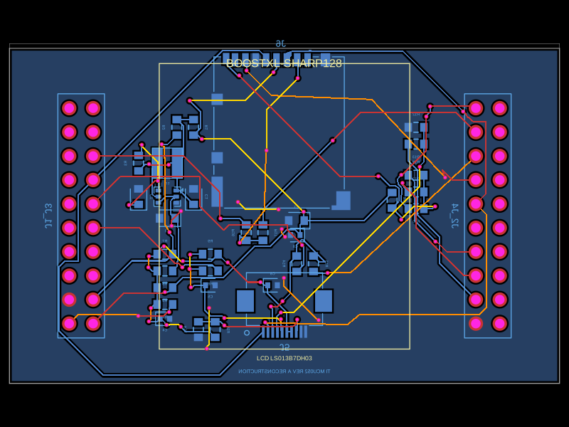 Similar packageabse/boostxl-sharp128This code defines a printed circuit board (PCB) with various surface-mount resistors, capacitors, inductors, and integrated circuits, including power management components and interface connectors, for a TI-based LCD and microSD module using 0603 and other package types.