tscircuit/boosters
This code defines PCB schematics, footprints, and 3D CAD models for various integrated circuits, connectors, sensors, and electronic components used in TI booster packs and modules.
- Version
- 0.1.19
- License
- unset
- Stars
- 0
boostxl-edumkii/index.circuit.tsx
PCB

Schematic

import { Fragment } from "react"
import type {
  CapacitorProps,
  LedProps,
  ResistorProps,
  TransistorProps,
} from "@tscircuit/props"
import { LIS3DHTR } from "./imports/LIS3DHTR"
import { OPA344NA_250 } from "./imports/OPA344NA_250"
import { OPT3001DNPR } from "./imports/OPT3001DNPR"
import { TMP117AIDRVR } from "./imports/TMP117AIDRVR"
import { YA13_FL7_4_B5Ka_45_10__R_Y06 } from "./imports/YA13_FL7_4_B5Ka_45_10__R_Y06"
import {
  boosterHeaderCadModel,
  buttonCadModel,
  buzzerCadModel,
  capacitor0603CadModel,
  capacitor0805CadModel,
  displayCadModel,
  greenLed0603CadModel,
  microphoneCadModel,
  redLed0603CadModel,
  resistor0603CadModel,
  rgbLedCadModel,
  servoHeaderCadModel,
  sod323CadModel,
  sot23CadModel,
} from "./imports/jlcCadModels"

const JlcResistor = (props: ResistorProps) => (
  <resistor {...props} cadModel={resistor0603CadModel} />
)

const JlcCapacitor = (props: CapacitorProps) => (
  <capacitor
    {...props}
    cadModel={
      props.footprint === "0805"
        ? capacitor0805CadModel
        : capacitor0603CadModel
    }
  />
)

const JlcTransistor = (props: TransistorProps) => (
  <transistor {...props} cadModel={sot23CadModel} />
)

const JlcLed = (props: LedProps) => (
  <led
    {...props}
    cadModel={
      props.color === "green" ? greenLed0603CadModel : redLed0603CadModel
    }
  />
)

const T = ({ from, to }: { from: string; to: string }) => {
  const netSelector = [from, to].find((selector) => selector.startsWith("net."))
  const netName = netSelector?.slice(4)

  return (
    <trace
      name={`${from} to ${to}`}
      from={from}
      to={to}
      schDisplayLabel={netName}
    />
  )
}

const pillOutline = (width: number, height: number, segments = 18) => {
  const radius = height / 2
  const straightHalfWidth = width / 2 - radius
  const points: Array<{ x: number; y: number }> = []

  for (let index = 0; index <= segments; index += 1) {
    const angle = Math.PI / 2 - (Math.PI * index) / segments
    points.push({
      x: straightHalfWidth + radius * Math.cos(angle),
      y: radius * Math.sin(angle),
    })
  }

  for (let index = 0; index <= segments; index += 1) {
    const angle = -Math.PI / 2 - (Math.PI * index) / segments
    points.push({
      x: -straightHalfWidth + radius * Math.cos(angle),
      y: radius * Math.sin(angle),
    })
  }

  return points
}

const boardOutline = pillOutline(127, 55.88)

const boosterHeaderFootprint = (
  <footprint>
    {Array.from({ length: 10 }, (_, index) => (
      <Fragment key={index}>
        <platedhole
          shape="circle"
          portHints={[`pin${index + 1}`]}
          pcbX={(index - 4.5) * 2.54}
          pcbY={0}
          holeDiameter="1mm"
          outerDiameter="1.8mm"
        />
      </Fragment>
    ))}
    <silkscreenrect
      pcbX={0}
      pcbY={0}
      width="24.86mm"
      height="2.3mm"
      filled={false}
      stroke="solid"
      strokeWidth="0.2mm"
    />
    <courtyardoutline
      outline={[
        { x: -12.43, y: -1.2 },
        { x: 12.43, y: -1.2 },
        { x: 12.43, y: 1.2 },
        { x: -12.43, y: 1.2 },
        { x: -12.43, y: -1.2 },
      ]}
    />
  </footprint>
)

const displayFootprint = (
  <footprint>
    {Array.from({ length: 10 }, (_, index) => (
      <Fragment key={index}>
        <smtpad
          portHints={[`pin${index + 1}`]}
          pcbX={-2.25 + index * 0.5}
          pcbY={0}
          width="0.3mm"
          height="1.4mm"
          shape="rect"
        />
      </Fragment>
    ))}
    <silkscreenrect
      pcbX={0}
      pcbY={-14.5}
      width="34mm"
      height="38mm"
      cornerRadius="1mm"
      filled={false}
      stroke="solid"
      strokeWidth="0.35mm"
    />
    <silkscreenrect
      pcbX={0}
      pcbY={-14.5}
      width="29mm"
      height="31mm"
      cornerRadius="0.5mm"
      filled={false}
      stroke="solid"
      strokeWidth="0.2mm"
    />
    <silkscreentext
      text="1.8in SPI TFT"
      pcbX={0}
      pcbY={-31.3}
      fontSize="1.1mm"
    />
    <courtyardoutline
      outline={[
        { x: -17.5, y: 1.5 },
        { x: 17.5, y: 1.5 },
        { x: 17.5, y: -34 },
        { x: -17.5, y: -34 },
        { x: -17.5, y: 1.5 },
      ]}
    />
  </footprint>
)

const buttonFootprint = (
  <footprint>
    <platedhole shape="circle" portHints={["pin1"]} pcbX={-3.25} pcbY={0} holeDiameter="1mm" outerDiameter="2mm" />
    <platedhole shape="circle" portHints={["pin2"]} pcbX={3.25} pcbY={0} holeDiameter="1mm" outerDiameter="2mm" />
    <hole pcbX={0} pcbY={-3.25} diameter="1.2mm" />
    <hole pcbX={0} pcbY={3.25} diameter="1.2mm" />
    <courtyardrect pcbX={0} pcbY={0} width="14.6mm" height="12.6mm" />
    {/* A path inherits the button's arbitrary PCB rotation. SilkscreenRect
        currently emits no rotation for angles other than 90-degree swaps. */}
    <silkscreenpath
      route={[
        { x: -6.2, y: -6.2 },
        { x: 6.2, y: -6.2 },
        { x: 6.2, y: 6.2 },
        { x: -6.2, y: 6.2 },
        { x: -6.2, y: -6.2 },
      ]}
      strokeWidth="0.3mm"
    />
    <silkscreencircle pcbX={0} pcbY={0} radius="3.5mm" isOutline strokeWidth="0.2mm" />
  </footprint>
)

const microphoneFootprint = (
  <footprint>
    <platedhole shape="circle" portHints={["pin1"]} pcbX={-1.9} pcbY={0} holeDiameter="0.9mm" outerDiameter="1.8mm" />
    <platedhole shape="circle" portHints={["pin2"]} pcbX={1.9} pcbY={0} holeDiameter="0.9mm" outerDiameter="1.8mm" />
    <courtyardcircle pcbX={0} pcbY={0} radius="5mm" />
    <silkscreencircle pcbX={0} pcbY={0} radius="4.8mm" isOutline strokeWidth="0.3mm" />
    <silkscreentext text="MIC" pcbX={0} pcbY={-5.8} fontSize="1mm" />
  </footprint>
)

const buzzerFootprint = (
  <footprint>
    <platedhole shape="circle" portHints={["pin1"]} pcbX={-3.75} pcbY={0} holeDiameter="0.9mm" outerDiameter="1.8mm" />
    <platedhole shape="circle" portHints={["pin2"]} pcbX={3.75} pcbY={0} holeDiameter="0.9mm" outerDiameter="1.8mm" />
    <courtyardcircle pcbX={0} pcbY={0} radius="6.2mm" />
    <silkscreencircle pcbX={0} pcbY={0} radius="6mm" isOutline strokeWidth="0.3mm" />
    <silkscreentext text="BUZZER" pcbX={0} pcbY={-7.1} fontSize="1mm" />
    <silkscreentext text="+" pcbX={-3.75} pcbY={2} fontSize="1.4mm" />
  </footprint>
)

const rgbFootprint = (
  <footprint>
    <smtpad portHints={["pin1"]} pcbX={-1.4} pcbY={-1.4} width="1.2mm" height="1.2mm" shape="rect" />
    <smtpad portHints={["pin2"]} pcbX={1.4} pcbY={-1.4} width="1.2mm" height="1.2mm" shape="rect" />
    <smtpad portHints={["pin3"]} pcbX={1.4} pcbY={1.4} width="1.2mm" height="1.2mm" shape="rect" />
    <smtpad portHints={["pin4"]} pcbX={-1.4} pcbY={1.4} width="1.2mm" height="1.2mm" shape="rect" />
    <silkscreenrect
      pcbX={0}
      pcbY={0}
      width="4.4mm"
      height="4.4mm"
      cornerRadius="0.5mm"
      filled={false}
      stroke="solid"
      strokeWidth="0.25mm"
    />
  </footprint>
)

export default () => (
  <board
    title="EDU BoosterPack TS"
    outline={boardOutline}
    layers={2}
    thickness="1.6mm"
    solderMaskColor="red"
    silkscreenColor="white"
    autorouter="auto-local"
    autorouterEffortLevel="5x"
    defaultTraceWidth="0.25mm"
    minTraceWidth="0.2mm"
    minViaHoleDiameter="0.3mm"
    minViaPadDiameter="0.45mm"
  >
    <schematicsheet name="Interface" displayName="Interface, Display & Controls" sheetIndex={1} />
    <schematicsheet name="Sensing" displayName="Sensors & Microphone" sheetIndex={2} />
    <schematicsheet name="Outputs" displayName="Outputs, Expansion & Power" sheetIndex={3} />

    <group name="InterfaceSheetSchematic" pcbX={0} pcbY={0} schSheetName="Interface" schX={0} schY={0}>
    <schematicsection name="Interface" displayName="LaunchPad Interface" />
    <schematicsection name="Display" displayName="SPI TFT Display" />
    <schematicsection name="Controls" displayName="Joystick & Buttons" />

    <silkscreentext text="EDU BOOSTERPACK TS" pcbX={0} pcbY={25.8} fontSize="1.6mm" />
    <silkscreentext text="LaunchPad XL compatible • 3V3 logic" pcbX={0} pcbY={23.7} fontSize="0.9mm" />
    <silkscreentext text="JOYSTICK" pcbX={-48} pcbY={20} fontSize="1mm" />
    <silkscreentext text="SENSORS" pcbX={5} pcbY={20} fontSize="1mm" />
    <silkscreentext text="BUTTONS" pcbX={49} pcbY={21.5} fontSize="1mm" />

    <group name="InterfaceSchematic" pcbX={0} pcbY={0} schX={-11.5} schY={0}>
    <pinheader
      name="J1"
      pinCount={10}
      pitch="2.54mm"
      gender="female"
      layer="bottom"
      pcbX={-22.86}
      pcbY={-1.27}
      pcbRotation={90}
      footprint={boosterHeaderFootprint}
      cadModel={boosterHeaderCadModel}
      showSilkscreenPinLabels
      pinLabels={["3V3", "JOY_X", "J1_3", "J1_4", "JOY_SEL", "MIC_IN", "LCD_SCLK", "LIGHT_INT", "I2C_SCL", "I2C_SDA"]}
      pinAttributes={{ pin3: { doNotConnect: true }, pin4: { doNotConnect: true } }}
      schSectionName="Interface"
      schX={-1.5}
      schY={1.5}
    />
    <pinheader
      name="J3"
      pinCount={10}
      pitch="2.54mm"
      gender="female"
      layer="bottom"
      pcbX={-20.32}
      pcbY={-1.27}
      pcbRotation={90}
      footprint={boosterHeaderFootprint}
      cadModel={null}
      showSilkscreenPinLabels
      pinLabels={["5V", "GND", "A23", "A24", "ACC_INT", "JOY_Y", "J3_27", "J3_28", "J3_29", "J3_30"]}
      pinAttributes={{
        pin3: { doNotConnect: true },
        pin4: { doNotConnect: true },
        pin7: { doNotConnect: true },
        pin8: { doNotConnect: true },
        pin9: { doNotConnect: true },
        pin10: { doNotConnect: true },
      }}
      schSectionName="Interface"
      schX={-1.5}
      schY={-1.5}
    />
    <pinheader
      name="J4"
      pinCount={10}
      pitch="2.54mm"
      gender="female"
      layer="bottom"
      pcbX={20.32}
      pcbY={-1.27}
      pcbRotation={90}
      footprint={boosterHeaderFootprint}
      cadModel={boosterHeaderCadModel}
      showSilkscreenPinLabels
      pinLabels={["LCD_DC", "BTN2", "BTN1", "GATOR", "J4_35", "J4_36", "RGB_B", "RGB_G", "RGB_R_BL", "BUZZER"]}
      pinAttributes={{ pin5: { doNotConnect: true }, pin6: { doNotConnect: true } }}
      schSectionName="Interface"
      schX={1.5}
      schY={-1.5}
    />
    <pinheader
      name="J2"
      pinCount={10}
      pitch="2.54mm"
      gender="female"
      layer="bottom"
      pcbX={22.86}
      pcbY={-1.27}
      pcbRotation={90}
      footprint={boosterHeaderFootprint}
      cadModel={null}
      showSilkscreenPinLabels
      pinLabels={["TEMP_INT", "J2_12", "LCD_CS", "J2_14", "LCD_MOSI", "J2_16", "LCD_RST", "J2_18", "SERVO_PWM", "GND"]}
      pinAttributes={{
        pin2: { doNotConnect: true },
        pin4: { doNotConnect: true },
        pin6: { doNotConnect: true },
        pin8: { doNotConnect: true },
      }}
      schSectionName="Interface"
      schX={1.5}
      schY={1.5}
    />

    <T from=".J1 > .pin1" to="net.V3V3" />
    <T from=".J1 > .pin2" to="net.JOY_X" />
    <T from=".J1 > .pin5" to="net.JOY_SEL" />
    <T from=".J1 > .pin6" to="net.MIC_IN" />
    <T from=".J1 > .pin7" to="net.LCD_SCLK" />
    <T from=".J1 > .pin8" to="net.LIGHT_INT" />
    <T from=".J1 > .pin9" to="net.I2C_SCL" />
    <T from=".J1 > .pin10" to="net.I2C_SDA" />
    <T from=".J3 > .pin1" to="net.V5V" />
    <T from=".J3 > .pin2" to="net.GND" />
    <T from=".J3 > .pin5" to="net.ACC_INT" />
    <T from=".J3 > .pin6" to="net.JOY_Y" />
    <T from=".J4 > .pin1" to="net.LCD_DC" />
    <T from=".J4 > .pin2" to="net.BTN2" />
    <T from=".J4 > .pin3" to="net.BTN1" />
    <T from=".J4 > .pin4" to="net.GATOR" />
    <T from=".J4 > .pin7" to="net.RGB_B" />
    <T from=".J4 > .pin8" to="net.RGB_G" />
    <T from=".J4 > .pin9" to="net.RGB_R_BL" />
    <T from=".J4 > .pin10" to="net.BUZZER" />
    <T from=".J2 > .pin1" to="net.TEMP_INT" />
    <T from=".J2 > .pin3" to="net.LCD_CS" />
    <T from=".J2 > .pin5" to="net.LCD_MOSI" />
    <T from=".J2 > .pin7" to="net.LCD_RST" />
    <T from=".J2 > .pin9" to="net.SERVO_PWM" />
    <T from=".J2 > .pin10" to="net.GND" />
    </group>

    <group name="DisplaySchematic" pcbX={0} pcbY={0} schX={-1.5} schY={0} schAutoLayoutEnabled>
    <chip
      name="U5"
      manufacturerPartNumber="1.8IN-ST7735-SPI-TFT"
      cadModel={displayCadModel}
      pinLabels={{
        pin1: ["GND1"],
        pin2: ["VCC"],
        pin3: ["SCLK"],
        pin4: ["MOSI"],
        pin5: ["RST"],
        pin6: ["DC"],
        pin7: ["CS"],
        pin8: ["BL"],
        pin9: ["MISO"],
        pin10: ["GND2"],
      }}
      noConnect={["MISO"]}
      pinAttributes={{
        pin1: { requiresGround: true },
        pin2: { requiresPower: true, requiresVoltage: "3.3V" },
        pin10: { requiresGround: true },
      }}
      footprint={displayFootprint}
      pcbX={0}
      pcbY={8}
      schSectionName="Display"
    />
    <JlcResistor name="R1" resistance="6.8" footprint="0603" pcbX={15} pcbY={20.5} schSectionName="Display" />
    <JlcCapacitor name="C4" capacitance="100nF" footprint="0603" pcbX={-12} pcbY={20.5} schSectionName="Display" />
    <JlcCapacitor name="C5" capacitance="10uF" footprint="0805" pcbX={-15.5} pcbY={20.5} schSectionName="Display" />
    <T from=".U5 > .GND1" to="net.GND" />
    <T from=".U5 > .GND2" to="net.GND" />
    <T from=".U5 > .VCC" to="net.V3V3" />
    <T from=".U5 > .SCLK" to="net.LCD_SCLK" />
    <T from=".U5 > .MOSI" to="net.LCD_MOSI" />
    <T from=".U5 > .RST" to="net.LCD_RST" />
    <T from=".U5 > .DC" to="net.LCD_DC" />
    <T from=".U5 > .CS" to="net.LCD_CS" />
    <T from=".U5 > .BL" to="net.LCD_BL" />
    <T from=".R1 > .pin1" to="net.LCD_BL" />
    <T from=".R1 > .pin2" to="net.RGB_R_BL" />
    <T from=".C4 > .pin1" to="net.V3V3" />
    <T from=".C4 > .pin2" to="net.GND" />
    <T from=".C5 > .pin1" to="net.V3V3" />
    <T from=".C5 > .pin2" to="net.GND" />
    </group>

    <group name="ControlsSchematic" pcbX={0} pcbY={0} schX={9.5} schY={-1} schAutoLayoutEnabled>
    <YA13_FL7_4_B5Ka_45_10__R_Y06
      name="U6"
      symbol={undefined}
      pinAttributes={{
        pin1: { requiresPower: true, requiresVoltage: "3.3V" },
        pin2: {},
        pin3: { requiresGround: true },
        pin4: { requiresPower: true, requiresVoltage: "3.3V" },
        pin5: {},
        pin6: { requiresGround: true },
        pin7: {},
        pin8: { requiresGround: true },
        pin9: { requiresGround: true },
        pin10: {},
        pin8_alt1: { requiresGround: true },
        pin7_alt1: {},
      }}
      pcbX={-40.64}
      pcbY={2.54}
      schSectionName="Controls"
    />
    <silkscreencircle pcbX={-40.64} pcbY={2.54} radius="10mm" isOutline strokeWidth="0.35mm" />
    <silkscreencircle pcbX={-40.64} pcbY={2.54} radius="7.2mm" isOutline strokeWidth="0.2mm" />
    <silkscreentext text="JOYSTICK" pcbX={-40.64} pcbY={-8.66} fontSize="1mm" />
    <JlcResistor name="R2" resistance="10k" footprint="0603" pcbX={-50} pcbY={-8} schSectionName="Controls" />
    <JlcCapacitor name="C6" capacitance="10nF" footprint="0603" pcbX={-51} pcbY={15} schSectionName="Controls" />
    <JlcCapacitor name="C7" capacitance="10nF" footprint="0603" pcbX={-47.5} pcbY={15.5} schSectionName="Controls" />
    <T from=".U6 > .pin1" to="net.V3V3" />
    <T from=".U6 > .pin2" to="net.JOY_X" />
    <T from=".U6 > .pin3" to="net.GND" />
    <T from=".U6 > .pin4" to="net.V3V3" />
    <T from=".U6 > .pin5" to="net.JOY_Y" />
    <T from=".U6 > .pin6" to="net.GND" />
    <T from=".U6 > .pin7" to="net.JOY_SEL" />
    <T from=".U6 > .pin8" to="net.GND" />
    <T from=".U6 > .pin9" to="net.GND" />
    <T from=".U6 > .pin10" to="net.JOY_SEL" />
    <T from=".R2 > .pin1" to="net.V3V3" />
    <T from=".R2 > .pin2" to="net.JOY_SEL" />
    <T from=".C6 > .pin1" to="net.JOY_X" />
    <T from=".C6 > .pin2" to="net.GND" />
    <T from=".C7 > .pin1" to="net.JOY_Y" />
    <T from=".C7 > .pin2" to="net.GND" />

    <pushbutton
      name="SW1"
      manufacturerPartNumber="MJTP1212"
      cadModel={buttonCadModel}
      pinLabels={{ pin1: ["SIG"], pin2: ["GND"] }}
      footprint={buttonFootprint}
      pcbX={48.26}
      pcbY={14}
      pcbRotation={-45}
      schSectionName="Controls"
    />
    <pushbutton
      name="SW2"
      manufacturerPartNumber="MJTP1212"
      cadModel={buttonCadModel}
      pinLabels={{ pin1: ["SIG"], pin2: ["GND"] }}
      footprint={buttonFootprint}
      pcbX={48.26}
      pcbY={-4.5}
      pcbRotation={-45}
      schSectionName="Controls"
    />
    <JlcResistor name="R3" resistance="10k" footprint="0603" pcbX={37} pcbY={13.5} schSectionName="Controls" />
    <JlcResistor name="R4" resistance="10k" footprint="0603" pcbX={36.5} pcbY={-4} schSectionName="Controls" />
    <T from=".SW1 > .SIG" to="net.BTN1" />
    <T from=".SW1 > .GND" to="net.GND" />
    <T from=".R3 > .pin1" to="net.V3V3" />
    <T from=".R3 > .pin2" to="net.BTN1" />
    <T from=".SW2 > .SIG" to="net.BTN2" />
    <T from=".SW2 > .GND" to="net.GND" />
    <T from=".R4 > .pin1" to="net.V3V3" />
    <T from=".R4 > .pin2" to="net.BTN2" />
    </group>
    </group>

    <group name="SensingSheetSchematic" pcbX={0} pcbY={0} schSheetName="Sensing" schX={0} schY={0}>
    <schematicsection name="Sensors" displayName="Environmental & Motion Sensors" />
    <schematicsection name="Audio" displayName="Microphone Front End" />
    <group name="SensorsSchematic" pcbX={0} pcbY={0} schX={-3.3} schY={-0.4} schAutoLayoutEnabled>
    <JlcResistor name="R5" resistance="10k" footprint="0603" pcbX={-9} pcbY={20.5} schSectionName="Sensors" />
    <JlcResistor name="R6" resistance="10k" footprint="0603" pcbX={-6} pcbY={20.5} schSectionName="Sensors" />
    <T from=".R5 > .pin1" to="net.V3V3" />
    <T from=".R5 > .pin2" to="net.I2C_SCL" />
    <T from=".R6 > .pin1" to="net.V3V3" />
    <T from=".R6 > .pin2" to="net.I2C_SDA" />

    <OPT3001DNPR
      name="U1"
      pcbX={-1}
      pcbY={20.5}
      schSectionName="Sensors"
    />
    <JlcCapacitor name="C1" capacitance="100nF" footprint="0603" pcbX={2.5} pcbY={20.5} schSectionName="Sensors" />
    <tracehint for=".U1 > .INT" offset={{ x: -1.2, y: -1.2 }} />
    <T from=".U1 > .VDD" to="net.V3V3" />
    <T from=".U1 > .ADDR" to="net.GND" />
    <T from=".U1 > .GND" to="net.GND" />
    <T from=".U1 > .EP" to="net.GND" />
    <T from=".U1 > .SCL" to="net.I2C_SCL" />
    <T from=".U1 > .SDA" to="net.I2C_SDA" />
    <T from=".U1 > .INT" to="net.LIGHT_INT" />
    <T from=".C1 > .pin1" to="net.V3V3" />
    <T from=".C1 > .pin2" to="net.GND" />

    <TMP117AIDRVR
      name="U2"
      pcbX={7}
      pcbY={20.5}
      schSectionName="Sensors"
    />
    <JlcCapacitor name="C2" capacitance="100nF" footprint="0603" pcbX={11} pcbY={20.5} schSectionName="Sensors" />
    <T from=".U2 > .V_POS" to="net.V3V3" />
    <T from=".U2 > .GND" to="net.GND" />
    <T from=".U2 > .EP" to="net.GND" />
    <T from=".U2 > .ADD0" to="net.GND" />
    <T from=".U2 > .SCL" to="net.I2C_SCL" />
    <T from=".U2 > .SDA" to="net.I2C_SDA" />
    <T from=".U2 > .ALERT" to="net.TEMP_INT" />
    <T from=".C2 > .pin1" to="net.V3V3" />
    <T from=".C2 > .pin2" to="net.GND" />

    <LIS3DHTR
      name="U3"
      pcbX={31.75}
      pcbY={5.1}
      schSectionName="Sensors"
      noConnect={["NC1", "NC2", "INT2", "RES", "ADC1", "ADC2", "ADC3"]}
    />
    <JlcCapacitor name="C3" capacitance="100nF" footprint="0603" pcbX={36.5} pcbY={5.1} schSectionName="Sensors" />
    <T from=".U3 > .VDD_IO" to="net.V3V3" />
    <T from=".U3 > .VDD" to="net.V3V3" />
    <T from=".U3 > .GND1" to="net.GND" />
    <T from=".U3 > .GND2" to="net.GND" />
    <T from=".U3 > .CS" to="net.V3V3" />
    <T from=".U3 > .pin4" to="net.I2C_SCL" />
    <T from=".U3 > .pin6" to="net.I2C_SDA" />
    <T from=".U3 > .pin7" to="net.GND" />
    <T from=".U3 > .INT1" to="net.ACC_INT" />
    <T from=".C3 > .pin1" to="net.V3V3" />
    <T from=".C3 > .pin2" to="net.GND" />
    </group>

    <group name="AudioSchematic" pcbX={0} pcbY={0} schX={6.3} schY={-0.1} schAutoLayoutEnabled>
    <chip
      name="U7"
      manufacturerPartNumber="CMA-4544PF-W"
      cadModel={microphoneCadModel}
      pinLabels={{ pin1: ["POS"], pin2: ["NEG"] }}
      pinAttributes={{
        pin1: { requiresPower: true },
        pin2: { requiresGround: true },
      }}
      footprint={microphoneFootprint}
      pcbX={-30.48}
      pcbY={-21.59}
      schSectionName="Audio"
    />
    <OPA344NA_250
      name="U4"
      pcbX={-31}
      pcbY={-13.8}
      pcbRotation={90}
      schSectionName="Audio"
    />
    <JlcResistor name="R7" resistance="2.2k" footprint="0603" pcbX={-36.5} pcbY={-18.5} schSectionName="Audio" />
    <JlcCapacitor name="C8" capacitance="1uF" footprint="0603" pcbX={-34.5} pcbY={-12.5} schSectionName="Audio" />
    <JlcResistor name="R8" resistance="100k" footprint="0603" pcbX={-27.5} pcbY={-9} schSectionName="Audio" />
    <JlcResistor name="R9" resistance="100k" footprint="0603" pcbX={-27.5} pcbY={-12} schSectionName="Audio" />
    <JlcCapacitor name="C9" capacitance="1uF" footprint="0603" pcbX={-22} pcbY={-18.5} schSectionName="Audio" />
    <JlcResistor name="R10" resistance="100k" footprint="0603" pcbX={-31} pcbY={-9} schSectionName="Audio" />
    <JlcResistor name="R11" resistance="10k" footprint="0603" pcbX={-26} pcbY={-15.8} schSectionName="Audio" />
    <JlcCapacitor name="C10" capacitance="100nF" footprint="0603" pcbX={-35} pcbY={-10} schSectionName="Audio" />
    <T from=".U7 > .POS" to="net.MIC_BIAS" />
    <T from=".R7 > .pin2" to="net.MIC_BIAS" />
    <T from=".R7 > .pin1" to="net.V3V3" />
    <T from=".U7 > .NEG" to="net.GND" />
    <T from=".C8 > .pin1" to="net.MIC_BIAS" />
    <T from=".C8 > .pin2" to="net.VREF" />
    <T from=".R8 > .pin1" to="net.V3V3" />
    <T from=".R8 > .pin2" to="net.VREF" />
    <T from=".R9 > .pin1" to="net.VREF" />
    <T from=".R9 > .pin2" to="net.GND" />
    <T from=".C9 > .pin1" to="net.VREF" />
    <T from=".C9 > .pin2" to="net.GND" />
    <T from=".U4 > .IN_POS" to="net.VREF" />
    <T from=".U4 > .IN_NEG" to="net.MIC_FB" />
    <T from=".R10 > .pin1" to="net.MIC_FB" />
    <T from=".R10 > .pin2" to="net.MIC_IN" />
    <T from=".R11 > .pin1" to="net.MIC_FB" />
    <T from=".R11 > .pin2" to="net.VREF" />
    <T from=".U4 > .V_POS" to="net.V3V3" />
    <T from=".U4 > .V_NEG" to="net.GND" />
    <T from=".U4 > .OUT" to="net.MIC_IN" />
    <T from=".C10 > .pin1" to="net.V3V3" />
    <T from=".C10 > .pin2" to="net.GND" />
    </group>
    </group>

    <group name="OutputsSheetSchematic" pcbX={0} pcbY={0} schSheetName="Outputs" schX={0} schY={0}>
    <schematicsection name="Outputs" displayName="RGB LED & Buzzer Drivers" />
    <schematicsection name="Expansion" displayName="Servo & Clip Expansion" />
    <schematicsection name="Power" displayName="Power Indicators" />
    <group name="OutputsSchematic" pcbX={0} pcbY={0} schX={-9.2} schY={0.5}>
    <chip
      name="U8"
      manufacturerPartNumber="CLV1A-FKB-CJ1M1F1BB7R4S3"
      cadModel={rgbLedCadModel}
      pinLabels={{ pin1: ["ANODE"], pin2: ["RED"], pin3: ["GREEN"], pin4: ["BLUE"] }}
      pinAttributes={{
        pin1: { requiresPower: true, requiresVoltage: "3.3V" },
        pin2: { requiresGround: true },
        pin3: { requiresGround: true },
        pin4: { requiresGround: true },
      }}
      footprint={rgbFootprint}
      pcbX={33}
      pcbY={-11.5}
      schX={-1}
      schY={1.3}
      schSectionName="Outputs"
    />
    <JlcResistor name="R12" resistance="330" footprint="0603" pcbX={37} pcbY={-9} schX={-4} schY={0.2} schSectionName="Outputs" />
    <JlcResistor name="R13" resistance="330" footprint="0603" pcbX={37} pcbY={-13} schX={2} schY={0.2} schSectionName="Outputs" />
    <JlcResistor name="R14" resistance="330" footprint="0603" pcbX={40} pcbY={-20} schX={5} schY={1.3} schSectionName="Outputs" />
    <JlcTransistor name="Q1" type="npn" footprint="sot23" pcbX={41} pcbY={-9} schX={-4} schY={-1.2} schSectionName="Outputs" />
    <JlcTransistor name="Q2" type="npn" footprint="sot23" pcbX={41} pcbY={-13} schX={0} schY={-1.2} schSectionName="Outputs" />
    <JlcTransistor name="Q3" type="npn" footprint="sot23" pcbX={41} pcbY={-17} schX={4} schY={-1.2} schSectionName="Outputs" />
    <JlcResistor name="R15" resistance="4.7k" footprint="0603" pcbX={37} pcbY={-7} schX={-4} schY={-3.2} schSectionName="Outputs" />
    <JlcResistor name="R16" resistance="4.7k" footprint="0603" pcbX={45} pcbY={-13} schX={0} schY={-3.2} schSectionName="Outputs" />
    <JlcResistor name="R17" resistance="4.7k" footprint="0603" pcbX={45} pcbY={-17} schX={4} schY={-3.2} schSectionName="Outputs" />
    <T from=".U8 > .ANODE" to="net.V3V3" />
    <T from=".U8 > .RED" to="net.RGB_RED_LED" />
    <T from=".R12 > .pin1" to="net.RGB_RED_LED" />
    <T from=".R12 > .pin2" to="net.RGB_RED_SINK" />
    <T from=".Q1 > .collector" to="net.RGB_RED_SINK" />
    <T from=".Q1 > .emitter" to="net.GND" />
    <T from=".Q1 > .base" to="net.RGB_RED_BASE" />
    <T from=".R15 > .pin1" to="net.RGB_RED_BASE" />
    <T from=".R15 > .pin2" to="net.RGB_R_BL" />
    <T from=".U8 > .GREEN" to="net.RGB_GREEN_LED" />
    <T from=".R13 > .pin1" to="net.RGB_GREEN_LED" />
    <T from=".R13 > .pin2" to="net.RGB_GREEN_SINK" />
    <T from=".Q2 > .collector" to="net.RGB_GREEN_SINK" />
    <T from=".Q2 > .emitter" to="net.GND" />
    <T from=".Q2 > .base" to="net.RGB_GREEN_BASE" />
    <T from=".R16 > .pin1" to="net.RGB_GREEN_BASE" />
    <T from=".R16 > .pin2" to="net.RGB_G" />
    <T from=".U8 > .BLUE" to="net.RGB_BLUE_LED" />
    <T from=".R14 > .pin1" to="net.RGB_BLUE_LED" />
    <T from=".R14 > .pin2" to="net.RGB_BLUE_SINK" />
    <T from=".Q3 > .collector" to="net.RGB_BLUE_SINK" />
    <T from=".Q3 > .emitter" to="net.GND" />
    <T from=".Q3 > .base" to="net.RGB_BLUE_BASE" />
    <T from=".R17 > .pin1" to="net.RGB_BLUE_BASE" />
    <T from=".R17 > .pin2" to="net.RGB_B" />

    <chip
      name="U9"
      manufacturerPartNumber="CEM-1203"
      cadModel={buzzerCadModel}
      pinLabels={{ pin1: ["POS"], pin2: ["NEG"] }}
      pinAttributes={{
        pin1: { requiresPower: true, requiresVoltage: "5V" },
        pin2: { requiresGround: true },
      }}
      footprint={buzzerFootprint}
      pcbX={31.75}
      pcbY={-20.32}
      schX={1.5}
      schY={3.7}
      schSectionName="Outputs"
    />
    <JlcTransistor name="Q4" type="npn" footprint="sot23" pcbX={40} pcbY={-23} schX={7.5} schY={-1.2} schSectionName="Outputs" />
    <JlcResistor name="R18" resistance="2.2k" footprint="0603" pcbX={44} pcbY={-23} schX={7.5} schY={-3.2} schSectionName="Outputs" />
    <diode name="D1" footprint="sod323" cadModel={sod323CadModel} pcbX={37} pcbY={-26.5} schX={5} schY={3.7} schSectionName="Outputs" />
    <T from=".U9 > .POS" to="net.V5V" />
    <T from=".U9 > .NEG" to="net.BUZZER_SINK" />
    <T from=".Q4 > .collector" to="net.BUZZER_SINK" />
    <T from=".Q4 > .emitter" to="net.GND" />
    <T from=".Q4 > .base" to="net.BUZZER_BASE" />
    <T from=".R18 > .pin1" to="net.BUZZER_BASE" />
    <T from=".R18 > .pin2" to="net.BUZZER" />
    <T from=".D1 > .anode" to="net.BUZZER_SINK" />
    <T from=".D1 > .cathode" to="net.V5V" />
    </group>

    <group name="ExpansionSchematic" pcbX={0} pcbY={0} schX={3.3} schY={1} schAutoLayoutEnabled>
    <pinheader
      name="JSERVO"
      doNotPlace
      pinCount={3}
      pitch="2.54mm"
      gender="male"
      cadModel={servoHeaderCadModel}
      pcbX={39}
      pcbY={23}
      pcbRotation={0}
      pinLabels={["GND", "5V", "PWM"]}
      showSilkscreenPinLabels
      schSectionName="Expansion"
    />
    <T from=".JSERVO > .pin1" to="net.GND" />
    <T from=".JSERVO > .pin2" to="net.V5V" />
    <T from=".JSERVO > .pin3" to="net.SERVO_PWM" />

    <platedhole name="GND_CLIP_A" shape="circle" holeDiameter="2.4mm" outerDiameter="3.4mm" pcbX={-27.2} pcbY={22.86} connectsTo="net.GND" />
    <platedhole name="GND_CLIP_B" shape="circle" holeDiameter="2.4mm" outerDiameter="3.4mm" pcbX={-23.6} pcbY={22.86} connectsTo="net.GND" />
    <platedhole name="SIG_CLIP_A" shape="circle" holeDiameter="2.4mm" outerDiameter="3.4mm" pcbX={23.6} pcbY={22.86} connectsTo="net.GATOR" />
    <platedhole name="SIG_CLIP_B" shape="circle" holeDiameter="2.4mm" outerDiameter="3.4mm" pcbX={27.2} pcbY={22.86} connectsTo="net.GATOR" />
    <JlcResistor name="R19" resistance="10k" footprint="0603" pcbX={29} pcbY={18.5} schSectionName="Expansion" />
    <T from=".R19 > .pin1" to="net.V3V3" />
    <T from=".R19 > .pin2" to="net.GATOR" />
    <silkscreentext text="GND CLIP" pcbX={-25.4} pcbY={18.8} fontSize="0.9mm" />
    <silkscreentext text="TOUCH / CLIP" pcbX={25.4} pcbY={18.8} fontSize="0.9mm" />
    </group>

    <group name="PowerSchematic" pcbX={0} pcbY={0} schX={11} schY={0.6} schAutoLayoutEnabled>
    <JlcLed name="D3V3" color="green" footprint="0603" pcbX={-53} pcbY={-13} schSectionName="Power" />
    <JlcResistor name="R3V3" resistance="1k" footprint="0603" pcbX={-50} pcbY={-13} schSectionName="Power" />
    <JlcLed name="D5V" color="red" footprint="0603" pcbX={-53} pcbY={-18} schSectionName="Power" />
    <JlcResistor name="R5V" resistance="1k" footprint="0603" pcbX={-50} pcbY={-18} schSectionName="Power" />
    <T from="net.V3V3" to=".R3V3 > .pin1" />
    <T from=".R3V3 > .pin2" to="net.PWR_3V3_LED" />
    <T from=".D3V3 > .anode" to="net.PWR_3V3_LED" />
    <T from=".D3V3 > .cathode" to="net.GND" />
    <T from="net.V5V" to=".R5V > .pin1" />
    <T from=".R5V > .pin2" to="net.PWR_5V_LED" />
    <T from=".D5V > .anode" to="net.PWR_5V_LED" />
    <T from=".D5V > .cathode" to="net.GND" />
    <silkscreentext text="3V3" pcbX={-56} pcbY={-13} fontSize="0.9mm" />
    <silkscreentext text="5V" pcbX={-56} pcbY={-18} fontSize="0.9mm" />
    </group>
    </group>

    <copperpour layer="bottom" connectsTo="net.GND" clearance="0.25mm" boardEdgeMargin="0.4mm" />
  </board>
)
Related Packages
 More from this authortscircuit/autorouting-dataset-01This code manages the hardware and electronic components for circuit design and PCB layout, defining components like resistors, capacitors, transistors, connectors, and footprints, and providing tools for component placement, PCB topology, and electrical connections.
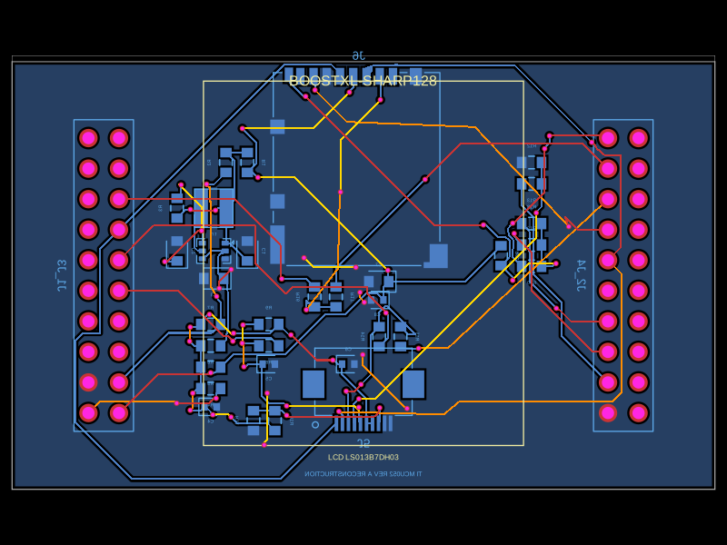 Similar packageabse/boostxl-sharp128This code defines a printed circuit board (PCB) with various surface-mount resistors, capacitors, inductors, and integrated circuits, including power management components and interface connectors, for a TI-based LCD and microSD module using 0603 and other package types.