tscircuit/boosters
This code defines PCB schematics, footprints, and 3D CAD models for various integrated circuits, connectors, sensors, and electronic components used in TI booster packs and modules.
- Version
- 0.1.19
- License
- unset
- Stars
- 0
boostxl-cc2650ma/index.circuit.tsx
PCB

Schematic

import { CC2650MODAMOHR } from "./imports/CC2650MODAMOHR"
import { FTSH_105_01_F_DV_K } from "./imports/FTSH_105_01_F_DV_K"
import { MX25R8035FZUIL0 } from "./imports/MX25R8035FZUIL0"
import { SSQ_110_23_L_D } from "./imports/SSQ_110_23_L_D"

const N = {
  V33: "net.V33",
  VDD: "net.VDD_CC2650M",
  GND: "net.GND",
  DIO0_TX: "net.DIO0_TX",
  DIO1_RX: "net.DIO1_RX",
  DIO2: "net.DIO2",
  DIO2_HDR: "net.DIO2_HDR",
  DIO3: "net.DIO3",
  DIO3_HDR: "net.DIO3_HDR",
  DIO4: "net.DIO4",
  DIO4_HDR: "net.DIO4_HDR",
  DIO5: "net.DIO5",
  DIO5_HDR: "net.DIO5_HDR",
  DIO6: "net.DIO6",
  DIO6_HDR: "net.DIO6_HDR",
  DIO7: "net.DIO7_MRDY",
  DIO7_HDR: "net.DIO7_HDR",
  DIO8: "net.DIO8_SRDY",
  DIO8_HDR: "net.DIO8_HDR",
  DIO9: "net.DIO9_CS",
  CS: "net.CS",
  DIO10: "net.DIO10_CLK",
  DIO11: "net.DIO11_MOSI",
  DIO12: "net.DIO12_MISO",
  DIO13: "net.DIO13",
  DIO14: "net.DIO14",
  DIO14_HDR: "net.DIO14_HDR",
  JTAG_TMS: "net.JTAG_TMS",
  JTAG_TCK: "net.JTAG_TCK",
  NRESET: "net.NRESET",
  LP_RESET: "net.LP_RESET",
  LEGACY_RESET: "net.LEGACY_RESET",
  LED_GREEN: "net.LED_GREEN",
  LED_RED: "net.LED_RED",
  FLASH_WP: "net.FLASH_WP",
  FLASH_HOLD: "net.FLASH_HOLD",
} as const

const verticalPinStyle = (pins: number[], margin: string) =>
  Object.fromEntries(
    pins.map((pin) => [
      `pin${pin}`,
      { marginTop: margin, marginBottom: margin },
    ]),
  )

const horizontalPinStyle = (pins: number[], margin: string) =>
  Object.fromEntries(
    pins.map((pin) => [
      `pin${pin}`,
      { marginLeft: margin, marginRight: margin },
    ]),
  )

const HEADER_PIN_STYLE = verticalPinStyle(
  Array.from({ length: 20 }, (_, index) => index + 1),
  "0.18mm",
)

const MODULE_PIN_STYLE = {
  ...verticalPinStyle(
    [2, 4, 5, 6, 7, 8, 9, 10, 11, 12, 13, 14, 15, 16, 17, 18, 19, 20, 21, 24],
    "0.16mm",
  ),
  ...horizontalPinStyle([22, 23], "0.35mm"),
  ...horizontalPinStyle([1, 3, 25, 26, 27, 28, 29], "0.18mm"),
}

const DEBUG_HEADER_PIN_STYLE = verticalPinStyle(
  Array.from({ length: 10 }, (_, index) => index + 1),
  "0.15mm",
)

const FLASH_PIN_STYLE = verticalPinStyle(
  Array.from({ length: 9 }, (_, index) => index + 1),
  "0.15mm",
)

export default function Circuit() {
  return (
    <board
      name="BOOSTXL_CC2650MA"
      width="75.3mm"
      height="28mm"
      outline={[
        { x: -37.65, y: -14 },
        { x: 37.65, y: -14 },
        { x: 37.65, y: 14 },
        { x: -37.65, y: 14 },
      ]}
      layers={2}
      solderMaskColor="red"
      silkscreenColor="white"
      defaultTraceWidth="0.15mm"
      minTraceWidth="0.15mm"
      minViaHoleDiameter="0.2mm"
      minViaPadDiameter="0.45mm"
      autorouter={{
        preset: "auto_local",
        local: true,
        traceClearance: "0.15mm",
      }}
      autorouterEffortLevel="5x"
      // TI's original component centroids are tighter than tscircuit's generic
      // courtyard estimates. Preserve those source placements and still route.
      placementDrcChecksDisabled
    >
      <schematicsheet
        name="radio-interface"
        displayName="CC2650 Module and LaunchPad Interface"
        sheetIndex={1}
      />
      <schematicsheet
        name="debug-flash"
        displayName="JTAG and Optional External Flash"
        sheetIndex={2}
      />
      <schematicsheet
        name="power-status"
        displayName="Power, Test Points, and Status LEDs"
        sheetIndex={3}
      />

      <group
        name="RADIO_INTERFACE"
        schSheetName="radio-interface"
        schX={0}
        schY={0}
        pcbX={0}
        pcbY={0}
        schMaxTraceDistance="1.1mm"
        schTraceAutoLabelEnabled
      >
        <schematictext
          text="CC2650MODA + BoosterPack interface"
          schX={-14.5}
          schY={8.8}
          fontSize={0.3}
          anchor="center_left"
        />

        <SSQ_110_23_L_D
          name="J1"
          layer="bottom"
          schX={-9}
          schY={1.5}
          schWidth="5.8mm"
          schHeight="10.5mm"
          schPinStyle={HEADER_PIN_STYLE}
          schPinArrangement={{
            leftSide: {
              pins: [1, 3, 5, 7, 9, 11, 13, 15, 17, 19],
              direction: "top-to-bottom",
            },
            rightSide: {
              pins: [2, 4, 6, 8, 10, 12, 14, 16, 18, 20],
              direction: "top-to-bottom",
            },
          }}
          pcbX={-12.997}
          pcbY={0.03}
          pcbRotation={90}
          noConnect={["pin2", "pin4", "pin6", "pin8", "pin10", "pin12", "pin14", "pin16", "pin18", "pin20"]}
          connections={{
            pin1: N.V33,
            pin3: N.DIO7_HDR,
            pin5: N.DIO0_TX,
            pin7: N.DIO1_RX,
            pin9: N.DIO2_HDR,
            pin11: N.DIO3_HDR,
            pin13: N.DIO10,
            pin15: N.DIO4_HDR,
            pin17: N.DIO5_HDR,
            pin19: N.DIO6_HDR,
          }}
        />

        <CC2650MODAMOHR
          name="U2"
          schX={0}
          schY={1}
          schWidth="7.4mm"
          schHeight="11.5mm"
          schPinStyle={MODULE_PIN_STYLE}
          schPinArrangement={{
            leftSide: {
              pins: [4, 5, 6, 7, 8, 11, 12, 14, 15, 16, 17, 18, 19, 20, 21],
              direction: "top-to-bottom",
            },
            rightSide: {
              pins: [9, 10, 13, 2, 24],
              direction: "top-to-bottom",
            },
            topSide: {
              pins: [22, 23],
              direction: "left-to-right",
            },
            bottomSide: {
              pins: [1, 3, 25, 26, 27, 28, 29],
              direction: "left-to-right",
            },
          }}
          pcbX={-25.6}
          pcbY={0.85}
          pcbRotation={90}
          internallyConnectedPins={[
            ["pin1", "pin3", "pin25", "pin26", "pin27", "pin28", "pin29"],
            ["pin22", "pin23"],
          ]}
          noConnect={["pin2", "pin24"]}
          connections={{
            pin1: N.GND,
            pin3: N.GND,
            pin4: N.DIO0_TX,
            pin5: N.DIO1_RX,
            pin6: N.DIO2,
            pin7: N.DIO3,
            pin8: N.DIO4,
            pin9: N.JTAG_TMS,
            pin10: N.JTAG_TCK,
            pin11: N.DIO5,
            pin12: N.DIO6,
            pin13: N.NRESET,
            pin14: N.DIO7,
            pin15: N.DIO8,
            pin16: N.DIO9,
            pin17: N.DIO10,
            pin18: N.DIO11,
            pin19: N.DIO12,
            pin20: N.DIO13,
            pin21: N.DIO14,
            pin22: N.VDD,
            pin23: N.VDD,
            pin25: N.GND,
            pin26: N.GND,
            pin27: N.GND,
            pin28: N.GND,
            pin29: N.GND,
          }}
        />

        <SSQ_110_23_L_D
          name="J2"
          layer="bottom"
          schX={8.2}
          schY={1.5}
          schWidth="5.8mm"
          schHeight="10.5mm"
          schPinStyle={HEADER_PIN_STYLE}
          schPinArrangement={{
            leftSide: {
              pins: [1, 3, 5, 7, 9, 11, 13, 15, 17, 19],
              direction: "top-to-bottom",
            },
            rightSide: {
              pins: [2, 4, 6, 8, 10, 12, 14, 16, 18, 20],
              direction: "top-to-bottom",
            },
          }}
          pcbX={30.203}
          pcbY={0.03}
          pcbRotation={90}
          noConnect={["pin1", "pin3", "pin5", "pin7", "pin8", "pin9", "pin13", "pin15", "pin17", "pin19"]}
          connections={{
            pin2: N.GND,
            pin4: N.DIO8_HDR,
            pin6: N.CS,
            pin10: N.LP_RESET,
            pin11: N.NRESET,
            pin12: N.DIO11,
            pin14: N.DIO12,
            pin16: N.DIO13,
            pin18: N.DIO14_HDR,
            pin20: N.LEGACY_RESET,
          }}
        />

        <resistor name="R9" resistance="0ohm" footprint="0603" manufacturerPartNumber="CRCW06030000Z0EC" schX={3} schY={-5} pcbX={-2.35} pcbY={-1.3} pcbRotation={180} connections={{ pin1: N.DIO7_HDR, pin2: N.DIO7 }} />
        <resistor name="R13" resistance="0ohm" footprint="0603" manufacturerPartNumber="CRCW06030000Z0EC" schX={3} schY={-6.9} pcbX={-2.35} pcbY={1.4} connections={{ pin1: N.DIO8, pin2: N.DIO8_HDR }} />
        <resistor name="R17" resistance="0ohm" footprint="0603" manufacturerPartNumber="CRCW06030000Z0EC" schX={9} schY={-6.9} pcbX={16.15} pcbY={-7.9} connections={{ pin1: N.NRESET, pin2: N.NRESET }} />
        <resistor name="R20" resistance="0ohm" footprint="0603" manufacturerPartNumber="CRCW06030000Z0EC" schX={3} schY={-8.8} pcbX={-21.15} pcbY={7.4} connections={{ pin1: N.DIO9, pin2: N.CS }} />
        <group name="DNM_RADIO_OPTIONS" bomDisabled>
          <resistor name="R7" showAsTranslucentModel resistance="0ohm" footprint="0603" manufacturerPartNumber="DNM" schX={-9} schY={-5} pcbX={-2.35} pcbY={-3} pcbRotation={180} connections={{ pin1: N.DIO3_HDR, pin2: N.DIO3 }} />
          <resistor name="R8" showAsTranslucentModel resistance="0ohm" footprint="0603" manufacturerPartNumber="DNM" schX={-3} schY={-5} pcbX={-2.45} pcbY={-9.2} connections={{ pin1: N.DIO2_HDR, pin2: N.DIO2 }} />
          <resistor name="R10" showAsTranslucentModel resistance="0ohm" footprint="0603" manufacturerPartNumber="DNM" schX={9} schY={-5} pcbX={-2.35} pcbY={-4.4} connections={{ pin1: N.DIO4_HDR, pin2: N.DIO4 }} />
          <resistor name="R11" showAsTranslucentModel resistance="0ohm" footprint="0603" manufacturerPartNumber="DNM" schX={-9} schY={-6.9} pcbX={-2.45} pcbY={-6.1} connections={{ pin1: N.DIO5_HDR, pin2: N.DIO5 }} />
          <resistor name="R12" showAsTranslucentModel resistance="0ohm" footprint="0603" manufacturerPartNumber="DNM" schX={-3} schY={-6.9} pcbX={-2.45} pcbY={-7.7} connections={{ pin1: N.DIO6_HDR, pin2: N.DIO6 }} />
          <resistor name="R18" showAsTranslucentModel resistance="0ohm" footprint="0603" manufacturerPartNumber="DNM" schX={-9} schY={-8.8} pcbX={16.15} pcbY={-9.333} pcbRotation={180} connections={{ pin1: N.LP_RESET, pin2: N.NRESET }} />
          <resistor name="R19" showAsTranslucentModel resistance="0ohm" footprint="0603" manufacturerPartNumber="DNM" schX={-3} schY={-8.8} pcbX={16.15} pcbY={-10.766} pcbRotation={180} connections={{ pin1: N.LEGACY_RESET, pin2: N.NRESET }} />
          <resistor name="R21" showAsTranslucentModel resistance="0ohm" footprint="0603" manufacturerPartNumber="DNM" schX={9} schY={-8.8} pcbX={16.15} pcbY={-12.199} pcbRotation={180} connections={{ pin1: N.LEGACY_RESET, pin2: N.DIO9 }} />
          <resistor name="R22" showAsTranslucentModel resistance="0ohm" footprint="0603" manufacturerPartNumber="DNM" schX={-3} schY={-10} pcbX={1.55} pcbY={-9.4} pcbRotation={180} connections={{ pin1: N.V33, pin2: N.DIO5 }} />
          <resistor name="R23" showAsTranslucentModel resistance="0ohm" footprint="0603" manufacturerPartNumber="DNM" schX={3} schY={-10} pcbX={1.55} pcbY={-10.65} pcbRotation={180} connections={{ pin1: N.V33, pin2: N.DIO6 }} />
        </group>
      </group>

      <group
        name="DEBUG_AND_FLASH"
        schSheetName="debug-flash"
        schX={0}
        schY={0}
        pcbX={0}
        pcbY={0}
        schMaxTraceDistance="1.1mm"
        schTraceAutoLabelEnabled
      >
        <schematicsection name="JTAG" displayName="1.27 mm JTAG Debug Header" sectionTitleFontSize="0.2mm" />
        <FTSH_105_01_F_DV_K
          name="P20"
          schSectionName="JTAG"
          schX={-7}
          schY={2}
          schWidth="4mm"
          schHeight="5.5mm"
          schPinStyle={DEBUG_HEADER_PIN_STYLE}
          schPinArrangement={{
            leftSide: {
              pins: [1, 3, 5, 7, 9],
              direction: "top-to-bottom",
            },
            rightSide: {
              pins: [2, 4, 6, 8, 10],
              direction: "top-to-bottom",
            },
          }}
          pcbX={-23.39}
          pcbY={-8.8}
          pcbRotation={180}
          noConnect={["pin7"]}
          connections={{
            pin1: N.V33,
            pin2: N.JTAG_TMS,
            pin3: N.GND,
            pin4: N.JTAG_TCK,
            pin5: N.GND,
            pin6: N.DIO5,
            pin8: N.DIO6,
            pin9: N.GND,
            pin10: N.NRESET,
          }}
        />

        <schematicsection name="OPTIONAL_FLASH" displayName="Optional MX25R8035F Flash (DNM)" sectionTitleFontSize="0.2mm" />
        <group name="DNM_FLASH_OPTIONS" bomDisabled>
          <MX25R8035FZUIL0
            name="U3"
            showAsTranslucentModel
            schSectionName="OPTIONAL_FLASH"
            schX={5}
            schY={2}
            schWidth="4.8mm"
            schHeight="5.8mm"
            schPinStyle={FLASH_PIN_STYLE}
            schPinArrangement={{
              leftSide: {
                pins: [1, 3, 7, 4, 9],
                direction: "top-to-bottom",
              },
              rightSide: {
                pins: [8, 6, 5, 2],
                direction: "top-to-bottom",
              },
            }}
            pcbX={5.35}
            pcbY={-7.55}
            pcbRotation={270}
            connections={{
              pin1: N.DIO14,
              pin2: N.DIO12,
              pin3: N.FLASH_WP,
              pin4: N.GND,
              pin5: N.DIO11,
              pin6: N.DIO10,
              pin7: N.FLASH_HOLD,
              pin8: N.V33,
              pin9: N.GND,
            }}
          />
          <resistor name="R24" showAsTranslucentModel resistance="0ohm" footprint="0603" manufacturerPartNumber="DNM" schSectionName="OPTIONAL_FLASH" schX={1} schY={-2.5} pcbX={-2.3} pcbY={4.45} pcbRotation={180} connections={{ pin1: N.DIO14_HDR, pin2: N.DIO14 }} />
          <resistor name="R25" showAsTranslucentModel resistance="10kohm" footprint="0402" manufacturerPartNumber="DNM" schSectionName="OPTIONAL_FLASH" schX={4} schY={-2.5} pcbX={-5.85} pcbY={6.788} pcbRotation={270} connections={{ pin1: N.V33, pin2: N.DIO14 }} />
          <resistor name="R26" showAsTranslucentModel resistance="10kohm" footprint="0402" manufacturerPartNumber="DNM" schSectionName="OPTIONAL_FLASH" schX={7} schY={-2.5} pcbX={2.812} pcbY={-7.85} connections={{ pin1: N.V33, pin2: N.FLASH_WP }} />
          <resistor name="R27" showAsTranslucentModel resistance="10kohm" footprint="0402" manufacturerPartNumber="DNM" schSectionName="OPTIONAL_FLASH" schX={10} schY={-2.5} pcbX={7.75} pcbY={-6.862} pcbRotation={270} connections={{ pin1: N.V33, pin2: N.FLASH_HOLD }} />
        </group>
        <capacitor
          name="C1"
          capacitance="100nF"
          footprint="0402"
          manufacturerPartNumber="GRM155R70J104KA01D"
          schSectionName="OPTIONAL_FLASH"
          schX={13}
          schY={-2.5}
          pcbX={6.088}
          pcbY={-5.6}
          pcbRotation={180}
          connections={{ pin1: N.V33, pin2: N.GND }}
        />
      </group>

      <group
        name="POWER_AND_STATUS"
        schSheetName="power-status"
        schX={0}
        schY={0}
        pcbX={0}
        pcbY={0}
        schMaxTraceDistance="1.1mm"
        schTraceAutoLabelEnabled
      >
        <schematictext text="Removable current-measurement link" schX={-13.5} schY={6.2} fontSize={0.24} anchor="center_left" />
        <pinheader
          name="P2"
          pinCount={2}
          pitch="2.54mm"
          gender="male"
          manufacturerPartNumber="BB02-HC021-KB1-603000"
          holeDiameter="1.05mm"
          platedDiameter="1.8mm"
          schX={-7}
          schY={3}
          pcbX={-3.02}
          pcbY={11.4}
          pcbRotation={180}
          connections={{ pin1: N.VDD, pin2: N.V33 }}
        />
        <schematictext text="M1 SNT-100-BK-G shunt installed on P2" schX={-11} schY={0.5} fontSize={0.2} anchor="center_left" />
        <group name="DNM_CURRENT_LINK" bomDisabled>
          <resistor
            name="R16"
            showAsTranslucentModel
            resistance="0ohm"
            footprint="0603"
            manufacturerPartNumber="DNM"
            schX={-3}
            schY={3}
            pcbX={-2.75}
            pcbY={8.6}
            connections={{ pin1: N.V33, pin2: N.VDD }}
          />
        </group>

        <schematicsection name="STATUS_LEDS" displayName="DIO2 Green and DIO4 Red Status LEDs" sectionTitleFontSize="0.2mm" />
        <resistor name="R5" resistance="180ohm" footprint="0402" manufacturerPartNumber="CRCW0402180RJNED" schSectionName="STATUS_LEDS" schX={2} schY={3} pcbX={15.438} pcbY={10.9} pcbRotation={180} connections={{ pin1: N.LED_GREEN, pin2: N.DIO2 }} />
        <led name="CR1" color="green" footprint="0603" manufacturerPartNumber="LP L296-J2L2-25" schSectionName="STATUS_LEDS" schX={5} schY={3} pcbX={15.502} pcbY={11.999} pcbRotation={180} connections={{ pin1: N.LED_GREEN, pin2: N.GND }} />
        <resistor name="R6" resistance="220ohm" footprint="0402" manufacturerPartNumber="CRCW0402220RJNED" schSectionName="STATUS_LEDS" schX={8} schY={3} pcbX={10.988} pcbY={10.9} pcbRotation={180} connections={{ pin1: N.LED_RED, pin2: N.DIO4 }} />
        <led name="CR2" color="red" footprint="0603" manufacturerPartNumber="LS L296-P2Q2-1" schSectionName="STATUS_LEDS" schX={11} schY={3} pcbX={10.902} pcbY={11.999} pcbRotation={180} connections={{ pin1: N.LED_RED, pin2: N.GND }} />

        <schematicsection name="TEST_POINTS" displayName="Reference Test Points (TI MH1-MH3)" sectionTitleFontSize="0.2mm" />
        <testpoint name="TP1" displayName="MH1 GND" footprintVariant="through_hole" holeDiameter="1.1mm" padDiameter="1.8mm" schSectionName="TEST_POINTS" schX={2} schY={-2} pcbX={10.55} pcbY={-11.9} connections={{ pin1: N.GND }} />
        <testpoint name="TP2" displayName="MH2 3V3" footprintVariant="through_hole" holeDiameter="1.1mm" padDiameter="1.8mm" schSectionName="TEST_POINTS" schX={6} schY={-2} pcbX={-4.25} pcbY={6.6} connections={{ pin1: N.V33 }} />
        <testpoint name="TP3" displayName="MH3 VDD" footprintVariant="through_hole" holeDiameter="1.1mm" padDiameter="1.8mm" schSectionName="TEST_POINTS" schX={10} schY={-2} pcbX={-1.45} pcbY={6.6} connections={{ pin1: N.VDD }} />
      </group>

      <keepout shape="rect" width="6.2mm" height="18mm" pcbX={-34.4} pcbY={0.85} layers={["top", "bottom"]} />
      <keepout shape="rect" width="75mm" height="0.6mm" pcbX={0} pcbY={13.65} layers={["top", "bottom"]} />
      <keepout shape="rect" width="75mm" height="0.6mm" pcbX={0} pcbY={-13.65} layers={["top", "bottom"]} />
      <keepout shape="rect" width="0.6mm" height="27mm" pcbX={37.3} pcbY={0} layers={["top", "bottom"]} />
      <keepout shape="rect" width="0.6mm" height="27mm" pcbX={-37.3} pcbY={0} layers={["top", "bottom"]} />
      <copperpour layer="top" connectsTo={N.GND} clearance="0.15mm" boardEdgeMargin="0.5mm" />
      <copperpour layer="bottom" connectsTo={N.GND} clearance="0.15mm" boardEdgeMargin="0.5mm" />

      <silkscreentext text="CC2650 Module BoosterPack" pcbX={4} pcbY={7.8} fontSize="1mm" />
      <silkscreentext text="BOOSTXL-CC2650MA Rev 1.0" pcbX={5} pcbY={5.9} fontSize="0.65mm" />
      <silkscreentext text="ANTENNA - NO COPPER" pcbX={-33.5} pcbY={-9.5} pcbRotation={90} fontSize="0.55mm" />
      <silkscreentext text="CURRENT" pcbX={-3.1} pcbY={13} fontSize="0.55mm" />
      <silkscreentext text="RED DIO4" pcbX={10.8} pcbY={13} fontSize="0.5mm" />
      <silkscreentext text="GREEN DIO2" pcbX={15.6} pcbY={13} fontSize="0.5mm" />
    </board>
  )
}
Related Packages
 More from this authortscircuit/autorouting-dataset-01This code manages the hardware and electronic components for circuit design and PCB layout, defining components like resistors, capacitors, transistors, connectors, and footprints, and providing tools for component placement, PCB topology, and electrical connections.
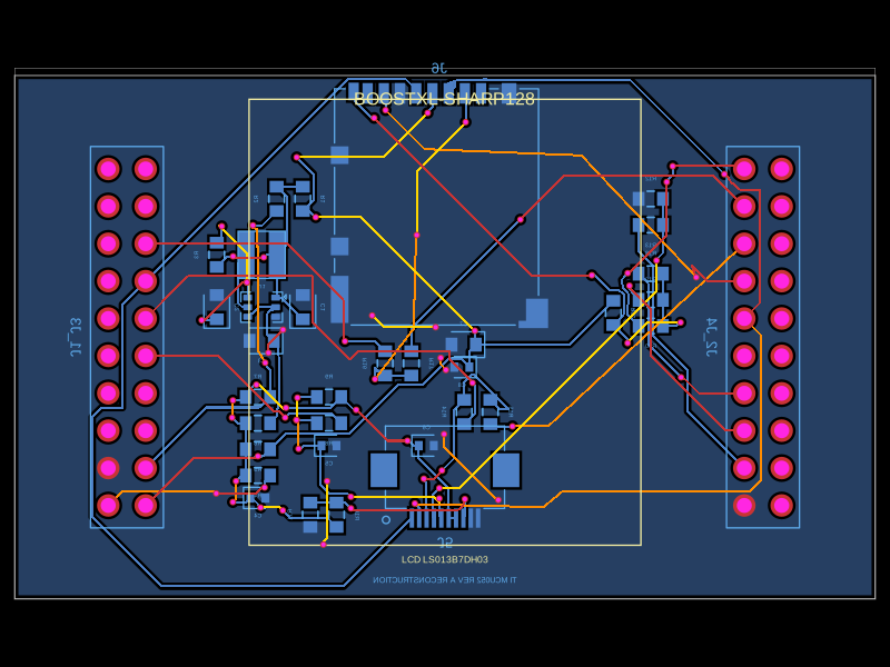 Similar packageabse/boostxl-sharp128This code defines a printed circuit board (PCB) with various surface-mount resistors, capacitors, inductors, and integrated circuits, including power management components and interface connectors, for a TI-based LCD and microSD module using 0603 and other package types.