techmannih/usbc-charger
This code defines a detailed electronic hardware design for an 85-265VAC to USB-C PD 18W wall charger, including the schematic layout and physical component placements such as connectors, filtering inductors, capacitors, resistors, protection diodes, and an isolated power module, all integrated with 3D models and mechanical enclosures.
- Version
- 1.0.7
- License
- unset
- Stars
- 0
index.circuit.tsx
PCB
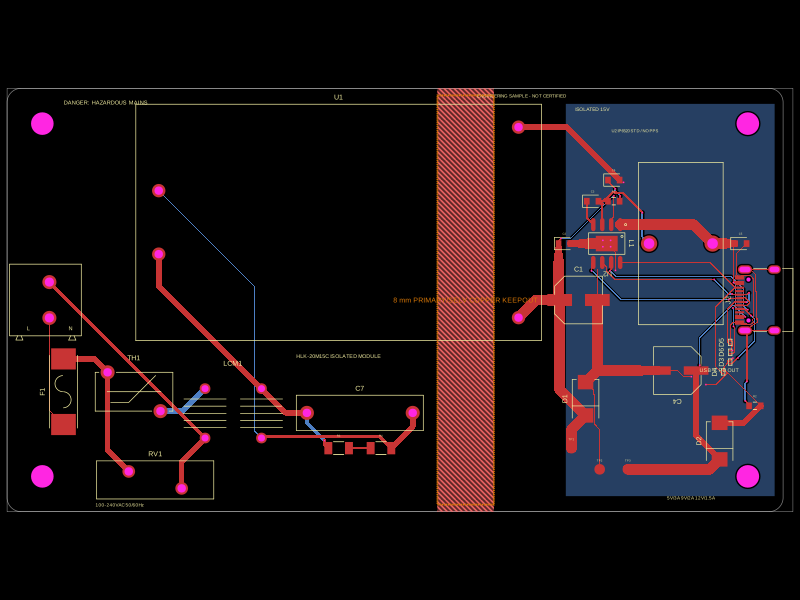
Schematic

import "tscircuit"
import { enclosure } from "tscircuit"

import { B32922C3104M189 } from "./imports/B32922C3104M189"
import { HLK_20M15C } from "./imports/HLK_20M15C"
import { IP6520StandardNonPps } from "./imports/IP6520"
import { MF72_5D9 } from "./imports/MF72_5D9"
import { MOV_14D471K } from "./imports/MOV_14D471K"
import { PDMTAT068125_220MLU } from "./imports/PDMTAT068125_220MLU"
import { PESD5V0H1BSF } from "./imports/PESD5V0H1BSF"
import { RVE100UF35V67RV0072 } from "./imports/RVE100UF35V67RV0072"
import { RVT1E101M0607 } from "./imports/RVT1E101M0607"
import { SCT1032T2A250V } from "./imports/SCT1032T2A250V"
import { SMBJ13A } from "./imports/SMBJ13A"
import { SMBJ15A } from "./imports/SMBJ15A"
import { TYPE_C_31_M_12 } from "./imports/TYPE_C_31_M_12"
import { WJ500V_5_08_2P } from "./imports/WJ500V_5_08_2P"
import { XRSQ1010_10mH_H } from "./imports/XRSQ1010_10mH_H"

/**
 * Engineering prototype for an 85-265 VAC to USB-C PD wall charger.
 *
 * The encapsulated HLK-20M15C module replaces the former custom flyback,
 * transformer and EMI magnetics. IP6520 converts its isolated 15 V output to
 * negotiated USB-PD source profiles: 5 V / 3 A, 9 V / 2 A and 12 V / 1.5 A
 * (18 W max). The exact standard IP6520 is the non-PPS variant; other IP6520
 * family variants are not approved substitutions.
 *
 * The 15 V / 1.333 A AC/DC module leaves limited conversion and thermal
 * headroom at the 18 W USB rating. Full-load thermal/efficiency testing,
 * including the 15 V to 12 V / 1.5 A operating point, is a hardware release
 * gate.
 * The carrier adds fused surge, inrush and common-mode filtering plus
 * secondary TVS/ESD protection. Physical safety and compliance remain subject
 * to accredited-laboratory testing of the final enclosure and production unit.
 */
export const UsbCPd18WWallCharger = () => (
  <>
    <board
      name="USB_C_PD_18W_WALL_CHARGER"
      title="85-265 VAC to USB-C PD 18 W Engineering Prototype"
      width="110mm"
      height="60mm"
      borderRadius="2mm"
      thickness="1.6mm"
      material="fr4"
      layers={2}
      isViaInPadAllowed
      solderMaskColor="#176b43"
      defaultTraceWidth="0.25mm"
      autorouterVersion="beta_pipeline9"
      autorouterEffortLevel="5x"
      schMaxTraceDistance="3mm"
    >
    <schematicsheet name="mains" displayName="AC Input and Isolated AC/DC Module" sheetIndex={1} />
    <schematicsheet name="pd" displayName="18 W USB-C PD Buck SoC Output" sheetIndex={2} />
    <schematicsection name="ac_input" displayName="Hazardous 85-265 VAC Input" />
    <schematicsection name="mains_filter" displayName="Fused Surge / Inrush / EMI Filter" />
    <schematicsection name="isolated_dc" displayName="Isolated 15 V Supply" />
    <schematicsection name="pd_output" displayName="USB-C PD Output" />

    {/* Four non-plated mounting holes support fixed enclosure standoffs. */}
    <hole name="H1" diameter="3.2mm" pcbX={-50} pcbY={25} />
    <hole name="H2" diameter="3.2mm" pcbX={-50} pcbY={-25} />
    <hole name="H3" diameter="3.2mm" pcbX={50} pcbY={25} />
    <hole name="H4" diameter="3.2mm" pcbX={50} pcbY={-25} />

    {/* The external mains lead must use a rated cable gland and strain relief. */}
    <WJ500V_5_08_2P
      name="J1"
      pcbX={-49}
      pcbY={0}
      pcbRotation={90}
      schSheetName="mains"
      schSectionName="ac_input"
      schX={-10.11}
      schY={1}
      connections={{ L: "net.AC_L", N: "net.AC_N" }}
    >
      <enclosure.cutoutaperture shape="circle" radius="4mm" margin="0.5mm" />
    </WJ500V_5_08_2P>
    <SCT1032T2A250V
      name="F1"
      pcbX={-47}
      pcbY={-13}
      pcbRotation={90}
      schSheetName="mains"
      schSectionName="ac_input"
      schX={-8.08}
      schY={1}
      connections={{ pin1: "net.AC_L", pin2: "net.AC_L_FUSED" }}
    />
    <MOV_14D471K
      name="RV1"
      pcbX={-34}
      pcbY={-25.5}
      schSheetName="mains"
      schSectionName="mains_filter"
      schX={-7}
      schY={-2}
      connections={{ pin1: "net.AC_L_FUSED", pin2: "net.AC_N" }}
    />
    <MF72_5D9
      name="TH1"
      pcbX={-37}
      pcbY={-13}
      schSheetName="mains"
      schSectionName="mains_filter"
      schX={-5.7}
      schY={1}
      connections={{ pin1: "net.AC_L_FUSED", pin2: "net.AC_L_LIMITED" }}
    />
    <XRSQ1010_10mH_H
      name="LCM1"
      pcbX={-23}
      pcbY={-16}
      schSheetName="mains"
      schSectionName="mains_filter"
      schX={-3}
      schY={1}
      connections={{
        pin1: "net.AC_L_LIMITED",
        pin2: "net.AC_L_FILTERED",
        pin3: "net.AC_N_FILTERED",
        pin4: "net.AC_N",
      }}
    />
    <B32922C3104M189
      name="C7"
      maxVoltageRating="305V"
      pcbX={-5}
      pcbY={-16}
      schSheetName="mains"
      schSectionName="mains_filter"
      schX={-1}
      schY={-2}
      connections={{ pin1: "net.AC_L_FILTERED", pin2: "net.AC_N_FILTERED" }}
    />
    {/* Two series 200 V resistors discharge the X2 capacitor C7 while sharing the mains voltage. */}
    <resistor
      name="R3"
      resistance="1Mohm"
      tolerance="1%"
      manufacturerPartNumber="1206W4F1004T5E"
      supplierPartNumbers={{ jlcpcb: ["C17927"] }}
      footprint="res1206"
      pcbX={-8}
      pcbY={-21}
      schSheetName="mains"
      schSectionName="mains_filter"
      schX={1}
      schY={-2.6}
      connections={{ pin1: "net.AC_L_FILTERED", pin2: "net.X_CAP_BLEED_MID" }}
    />
    <resistor
      name="R4"
      resistance="1Mohm"
      tolerance="1%"
      manufacturerPartNumber="1206W4F1004T5E"
      supplierPartNumbers={{ jlcpcb: ["C17927"] }}
      footprint="res1206"
      pcbX={-2}
      pcbY={-21}
      schSheetName="mains"
      schSectionName="mains_filter"
      schX={3}
      schY={-2}
      connections={{ pin1: "net.X_CAP_BLEED_MID", pin2: "net.AC_N_FILTERED" }}
    />
    <HLK_20M15C
      name="U1"
      pcbX={-8}
      pcbY={11}
      schSheetName="mains"
      schSectionName="isolated_dc"
      schX={2}
      schY={1}
      schWidth={1.865}
      schHeight={0.6}
      schPinArrangement={{
        leftSide: { direction: "top-to-bottom", pins: ["AC1", "AC2"] },
        rightSide: { direction: "top-to-bottom", pins: ["VOUT_15V", "GND"] },
      }}
      connections={{
        AC2: "net.AC_N_FILTERED",
        AC1: "net.AC_L_FILTERED",
        VOUT_15V: "net.VIN_15V",
        GND: "net.GND",
      }}
    />

    {/* Standard non-PPS IP6520 reference application: local input bulk and high-frequency bypass. */}
    <RVE100UF35V67RV0072
      name="C1"
      maxVoltageRating="35V"
      polarized
      pcbX={26}
      pcbY={0}
      schSheetName="pd"
      schSectionName="isolated_dc"
      schX={-8}
      schY={2.42}
      connections={{ pin1: "net.VIN_15V", pin2: "net.GND" }}
    />
    <capacitor
      name="C2"
      capacitance="100nF"
      maxVoltageRating="50V"
      manufacturerPartNumber="CC0603KRX7R9BB104"
      supplierPartNumbers={{ jlcpcb: ["C14663"] }}
      footprint="cap0603"
      pcbX={24}
      pcbY={8}
      schOrientation="vertical"
      schSheetName="pd"
      schSectionName="isolated_dc"
      schX={-6}
      schY={3}
      connections={{ pin1: "net.VIN_15V", pin2: "net.GND" }}
    />
    <SMBJ15A
      name="D1"
      pcbX={27}
      pcbY={-14}
      pcbRotation={90}
      schSheetName="pd"
      schSectionName="isolated_dc"
      schX={-4}
      schY={-1}
      schWidth={0.6}
      connections={{ C: "net.VIN_15V", A: "net.GND" }}
    />
    <IP6520StandardNonPps
      name="U2"
      pcbX={30}
      pcbY={8}
      pcbRotation={180}
      schSheetName="pd"
      schSectionName="pd_output"
      schX={0}
      schY={1}
      schWidth={1.865}
      schHeight={1}
      schPinArrangement={{
        leftSide: { direction: "top-to-bottom", pins: ["VIN", "BST", "CC1", "CC2"] },
        rightSide: { direction: "top-to-bottom", pins: ["SW", "VOUT", "DP", "DM", "GND"] },
      }}
      connections={{
        VIN: "net.VIN_15V",
        GND: "net.GND",
        SW: "net.SW",
        BST: "net.BST",
        VOUT: "net.VBUS_OUT",
        DM: "net.USB_DM",
        DP: "net.USB_DP",
        CC1: "net.CC1",
        CC2: "net.CC2",
      }}
    />
    <via name="U2_EP_1" pcbX={29.45} pcbY={7.55} connectsTo="net.GND" outerDiameter="0.55mm" holeDiameter="0.25mm" />
    <via name="U2_EP_2" pcbX={30.55} pcbY={7.55} connectsTo="net.GND" outerDiameter="0.55mm" holeDiameter="0.25mm" />
    <via name="U2_EP_3" pcbX={29.45} pcbY={8.45} connectsTo="net.GND" outerDiameter="0.55mm" holeDiameter="0.25mm" />
    <via name="U2_EP_4" pcbX={30.55} pcbY={8.45} connectsTo="net.GND" outerDiameter="0.55mm" holeDiameter="0.25mm" />
    <capacitor
      name="C3"
      capacitance="2.2uF"
      maxVoltageRating="25V"
      manufacturerPartNumber="GRM188Z71E225KE43D"
      supplierPartNumbers={{ jlcpcb: ["C415535"] }}
      footprint="cap0603"
      pcbX={28}
      pcbY={14}
      schOrientation="vertical"
      schSheetName="pd"
      schSectionName="pd_output"
      schX={3}
      schY={3}
      connections={{ pin1: "net.BST", pin2: "net.SW" }}
    />

    {/* Orderable 22 uH / 16 A, 8 mOhm buck inductor. The old EMI chokes were removed with the flyback stage. */}
    <PDMTAT068125_220MLU
      name="L1"
      pcbX={40.5}
      pcbY={8}
      pcbRotation={270}
      schSheetName="pd"
      schSectionName="pd_output"
      schX={4}
      schY={1}
      connections={{ pin1: "net.SW", pin2: "net.VBUS_OUT" }}
    />
    <resistor
      name="R1"
      resistance="2ohm"
      tolerance="1%"
      manufacturerPartNumber="FRC0603F2R00TS"
      supplierPartNumbers={{ jlcpcb: ["C2933191"] }}
      footprint="res0603"
      pcbX={31}
      pcbY={14}
      schSheetName="pd"
      schSectionName="pd_output"
      schX={2}
      schY={-1.42}
      connections={{ pin1: "net.SW", pin2: "net.SNUB" }}
    />
    <capacitor
      name="C6"
      capacitance="1nF"
      maxVoltageRating="50V"
      manufacturerPartNumber="GRM1885C1H102JA01D"
      supplierPartNumbers={{ jlcpcb: ["C77026"] }}
      footprint="cap0603"
      pcbX={31}
      pcbY={17}
      schOrientation="vertical"
      schSheetName="pd"
      schSectionName="pd_output"
      schX={4}
      schY={-2}
      connections={{ pin1: "net.SNUB", pin2: "net.GND" }}
    />

    {/* Output capacitors are rated above the highest 12 V PDO. */}
    <RVT1E101M0607
      name="C4"
      maxVoltageRating="25V"
      polarized
      pcbX={40}
      pcbY={-10}
      pcbRotation={180}
      schSheetName="pd"
      schSectionName="pd_output"
      schX={7}
      schY={2.42}
      connections={{ pin1: "net.VBUS_OUT", pin2: "net.GND" }}
    />
    <resistor
      name="R2"
      resistance="0ohm"
      manufacturerPartNumber="0603WAF0000T5E"
      supplierPartNumbers={{ jlcpcb: ["C21189"] }}
      footprint="res0603"
      pcbX={51}
      pcbY={-15}
      schSheetName="pd"
      schSectionName="pd_output"
      schX={14.5}
      schY={-2}
      schOrientation="vertical"
      connections={{ pin1: "net.USB_SHIELD", pin2: "net.GND" }}
    />
    <capacitor
      name="C5"
      capacitance="100nF"
      maxVoltageRating="50V"
      manufacturerPartNumber="CC0603KRX7R9BB104"
      supplierPartNumbers={{ jlcpcb: ["C14663"] }}
      footprint="cap0603"
      pcbX={49}
      pcbY={8}
      schOrientation="vertical"
      schSheetName="pd"
      schSectionName="pd_output"
      schX={9}
      schY={3}
      connections={{ pin1: "net.VBUS_OUT", pin2: "net.GND" }}
    />
    <SMBJ13A
      name="D2"
      pcbX={46}
      pcbY={-20}
      pcbRotation={90}
      schSheetName="pd"
      schSectionName="pd_output"
      schX={7}
      schY={-2.6}
      schWidth={0.6}
      connections={{ C: "net.VBUS_OUT", A: "net.GND" }}
    />
    {/* Low-capacitance bidirectional ESD clamps sit next to the exposed port. */}
    <PESD5V0H1BSF
      name="D3"
      pcbX={47.5}
      pcbY={-8.8}
      pcbRotation={90}
      schSheetName="pd"
      schSectionName="pd_output"
      schX={8.5}
      schY={-2}
      connections={{ pin1: "net.CC1", pin2: "net.GND" }}
    />
    <PESD5V0H1BSF
      name="D4"
      pcbX={46.5}
      pcbY={-10.2}
      pcbRotation={90}
      schSheetName="pd"
      schSectionName="pd_output"
      schX={9.81}
      schY={-2}
      connections={{ pin1: "net.CC2", pin2: "net.GND" }}
    />
    <PESD5V0H1BSF
      name="D5"
      pcbX={47.5}
      pcbY={-6}
      pcbRotation={90}
      schSheetName="pd"
      schSectionName="pd_output"
      schX={11.5}
      schY={-2}
      connections={{ pin1: "net.USB_DP", pin2: "net.GND" }}
    />
    <PESD5V0H1BSF
      name="D6"
      pcbX={47.5}
      pcbY={-7.4}
      pcbRotation={90}
      schSheetName="pd"
      schSectionName="pd_output"
      schX={13.29}
      schY={-2}
      connections={{ pin1: "net.USB_DM", pin2: "net.GND" }}
    />
    <TYPE_C_31_M_12
      name="J2"
      pcbX={51}
      pcbY={0}
      pcbRotation={90}
      schSheetName="pd"
      schSectionName="pd_output"
      schX={13}
      schY={1}
      connections={{
        CC1: "net.CC1",
        CC2: "net.CC2",
        DP1: "net.USB_DP",
        DP2: "net.USB_DP",
        DN1: "net.USB_DM",
        DN2: "net.USB_DM",
        VBUS1: "net.VBUS_OUT",
        VBUS2: "net.VBUS_OUT",
        GND1: "net.GND",
        GND2: "net.GND",
        SH1: "net.USB_SHIELD",
        SH2: "net.USB_SHIELD",
        SH3: "net.USB_SHIELD",
        SH4: "net.USB_SHIELD",
      }}
      noConnect={["SBU1", "SBU2"]}
    >
      <enclosure.cutoutaperture shape="pill" width="10mm" height="4mm" margin="0.25mm" />
    </TYPE_C_31_M_12>

    {/* Ground copper is restricted to the isolated low-voltage side. */}
    <copperpour
      name="ISOLATED_GND_BOTTOM"
      layer="bottom"
      connectsTo="net.GND"
      padMargin="0.2mm"
      traceMargin="0.15mm"
      outline={[{ x: 24, y: -28 }, { x: 54, y: -28 }, { x: 54, y: 28 }, { x: 24, y: 28 }]}
    />
    {/* An 8 mm all-layer copper-free corridor separates primary and SELV copper. */}
    <keepout shape="rect" layers={["top", "bottom"]} pcbX={10} pcbY={0} width="8mm" height="60mm" />
    <fabricationnoterect pcbX={10} pcbY={0} width="8mm" height="58mm" hasStroke isStrokeDashed strokeWidth={0.25} color="#d97706" />
    <fabricationnotetext text="8 mm PRIMARY/SELV COPPER KEEPOUT" pcbX={10} pcbY={0} fontSize="1mm" anchorAlignment="center" color="#d97706" />

    {/* Isolated-side test access for production and compliance measurements. */}
    <testpoint name="TP1" footprintVariant="pad" padShape="circle" padDiameter="1.5mm" pcbX={25} pcbY={-21} schSheetName="pd" schSectionName="isolated_dc" schX={-5} schY={-4} connections={{ pin1: "net.VIN_15V" }} />
    <testpoint name="TP2" footprintVariant="pad" padShape="circle" padDiameter="1.5mm" pcbX={29} pcbY={-24} schSheetName="pd" schSectionName="isolated_dc" schX={-3} schY={-4} connections={{ pin1: "net.GND" }} />
    <testpoint name="TP3" footprintVariant="pad" padShape="circle" padDiameter="1.5mm" pcbX={33} pcbY={-24} schSheetName="pd" schSectionName="pd_output" schX={5} schY={-4} connections={{ pin1: "net.VBUS_OUT" }} />

    <silkscreentext text="DANGER: HAZARDOUS MAINS" pcbX={-41} pcbY={28} fontSize="0.8mm" />
    <silkscreentext text="100-240VAC 50/60Hz" pcbX={-39} pcbY={-29} fontSize="0.65mm" />
    <silkscreentext text="L" pcbX={-52} pcbY={-4} fontSize="0.8mm" />
    <silkscreentext text="N" pcbX={-46} pcbY={-4} fontSize="0.8mm" />
    <silkscreentext text="HLK-20M15C ISOLATED MODULE" pcbX={-8} pcbY={-8} fontSize="0.75mm" />
    <silkscreentext text="ISOLATED 15V" pcbX={28} pcbY={27} fontSize="0.7mm" />
    <silkscreentext text="U2 IP6520 STD / NO PPS" pcbX={34} pcbY={24} fontSize="0.6mm" />
    <silkscreentext text="USB-C PD OUT" pcbX={46} pcbY={-10} fontSize="0.75mm" />
    <silkscreentext text="5V/3A  9V/2A  12V/1.5A" pcbX={42} pcbY={-28} fontSize="0.65mm" />
    </board>
    {/* Fit-check shell only. Production requires a lab-reviewed, flame-retardant enclosure. */}
    <enclosure.fdm.box
      boardRef=".USB_C_PD_18W_WALL_CHARGER"
      width="116mm"
      height="66mm"
      depth="42mm"
      wallThickness="2mm"
    />
  </>
)

export const UsbCPd18WCharger = UsbCPd18WWallCharger
export default UsbCPd18WWallCharger
Related Packages
 More from this authortechmannih/testsCreates a 10mm x 10mm circuit board featuring an axial battery component labeled U1 at the origin.
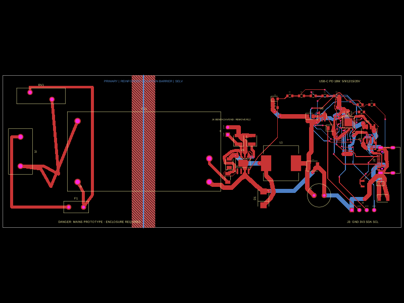 Similar packageseveibar/usbc-pd-chargerThis code defines and assembles a hardware schematic of an 18W USB-C PD wall charger with mains input, protection, high-voltage isolation, a DC buck converter with switching regulator, filtering, and USB-C output with ESD protection.
 Discover something newabse/boostxl-uln2003This code defines a React component that models a through-hole or surface-mount LED with specified pin labels, footprint, silkscreen, and 3D CAD model for PCB layout.